Method of selective coverage of high aspect ratio structures with a conformal film

a conformal film and high aspect ratio technology, applied in the direction of vacuum evaporation coating, coating, sputtering coating, etc., can solve the problems of high deposition rate, increase in the depth to width of features, and inability to provide void-free gap-filling in high aspect ratio features

Active Publication Date: 2009-12-01
NOVELLUS SYSTEMS
View PDF71 Cites 353 Cited by
  • Summary
  • Abstract
  • Description
  • Claims
  • Application Information

AI Technical Summary

Benefits of technology

[0012]The present invention provides methods for forming thin dielectric films by sele...

Problems solved by technology

However, as design rules continue to shrink, the aspect ratios (depth to width) of features increase, and traditional CVD techniques can no longer provide void-free gap-fill in these high aspect ratio features.
However, one drawback to ALD is that the deposition rates are very low.
These processes are unacceptably slow in some applications in the manufacturing environment.
However, the processes may fail to completely fill a structure, especially if ...

Method used


Image

  • Method of selective coverage of high aspect ratio structures with a conformal film
  • Method of selective coverage of high aspect ratio structures with a conformal film
  • Method of selective coverage of high aspect ratio structures with a conformal film

Examples


Embodiment Construction

[0024]In the following detailed description, numerous specific embodiments are set forth in order to provide a thorough understanding of the invention. However, as will be apparent to those skilled in the art, the present invention may be practiced without these specific details or by using alternate elements or processes. In other instances well-known processes, procedures and components have not been described in detail so as not to unnecessarily obscure aspects of the present invention.

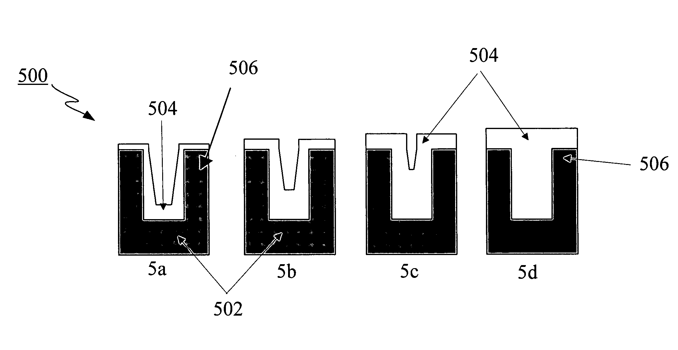
[0025]The method provided is well suited to a variety of semiconductor processing and other applications where control over film coverage is important, such as in the formation of a sacrificial mask over high aspect ratio gaps, or to achieve bottom-up gap fill of high aspect ratio gaps in a conformal dielectric deposition process such as PDL or ALD.

[0026]General Deposition Process Parameters

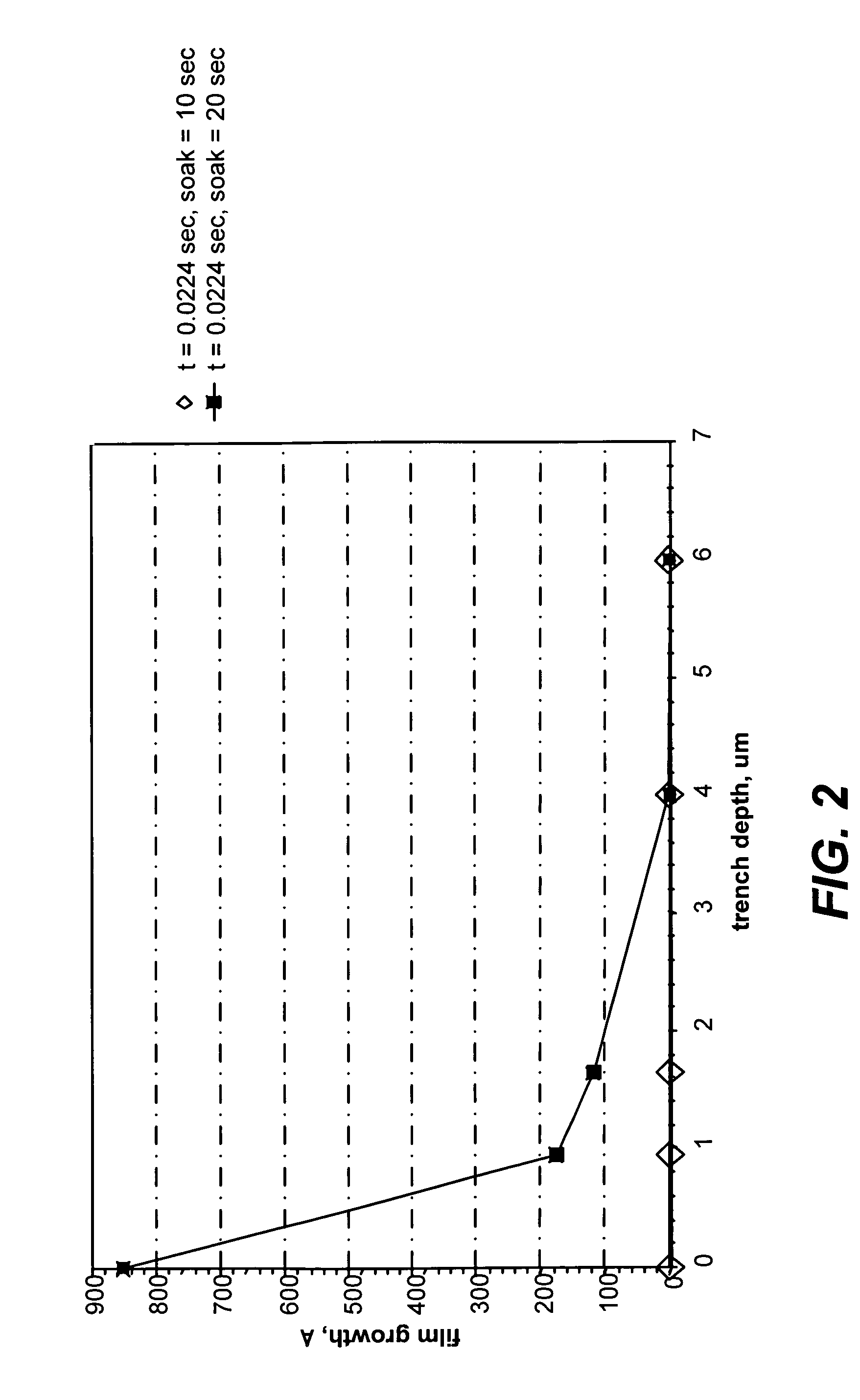
[0027]The dielectric deposition may be achieved using any suitable conformal process, for example ALD or PDL....


PUM

PropertyMeasurementUnit
Timeaaaaaaaaaa
Timeaaaaaaaaaa
Timeaaaaaaaaaa

Abstract

Methods for forming thin dielectric films by selectively depositing a conformal film of dielectric material on a high aspect ratio structure have uses in semiconductor processing and other applications. A method for forming a dielectric film involves providing in a deposition reaction chamber a substrate having a gap on the surface. The gap has a top opening and a surface area comprising a bottom and sidewalls running from the top to the bottom. A conformal silicon oxide-based dielectric film is selectively deposited in the gap by first preferentially applying a film formation catalyst or a catalyst precursor on a portion representing less than all of the gap surface area. The substrate surface is then exposed to a silicon-containing precursor gas such that a silicon oxide-based dielectric film layer is preferentially formed on the portion of the gap surface area. The preferential application of the catalyst or catalyst precursor may occur either at the top of the gap, for example to form a sacrificial mask, or at the bottom of the gap to create a seamless and void-free gap fill.

Description

FIELD OF THE INVENTION[0001]This invention relates to methods for forming thin dielectric films. More particularly, the invention pertains to methods for forming thin dielectric films by selectively depositing a conformal film of dielectric material on a high aspect ratio structure.BACKGROUND OF THE INVENTION[0002]Conformal, uniform dielectric films have many applications in semiconductor manufacturing. In the fabrication of sub-micron integrated circuits (ICs) several layers of dielectric film are deposited. Four such layers are shallow trench isolation (STI), premetal dielectric (PMD), inter-metal dielectric (IMD) and interlayer dielectric (ILD). All four of these layers require silicon dioxide films that fill features of various sizes and have uniform film thicknesses across the wafer.[0003]Chemical vapor deposition (CVD) has traditionally been the method of choice for depositing silicon dioxide films. However, as design rules continue to shrink, the aspect ratios (depth to width...

Claims


Application Information

Patent Timeline
IPC IPC(8): H01L21/44
CPCC23C14/046H01L21/02123H01L21/02164H01L21/02214H01L21/02312H01L21/31604H01L21/76224H01L21/0228H01L21/76837
Inventor PAPASOULIOTIS, GEORGE D.BURETEA, MIHAIMUI, COLLIN
Owner NOVELLUS SYSTEMS
Why Eureka
Try Eureka