Method for Increasing Oxide Etch Selectivity

Active Publication Date: 2016-01-21
TOKYO ELECTRON LTD
View PDF7 Cites 2 Cited by
  • Summary
  • Abstract
  • Description
  • Claims
  • Application Information

AI Technical Summary

Benefits of technology

[0004]In some microfabrication processes there can be multiple etch processes required for etching contact-like features through oxide materials and landing on (uncovering) source/drain materials. Such etch processes can be used to create both planar and three-dimensional transistor structures. Successfully executing some of these etch processes has been challenging because of poor selectivity associated with conventional etch techniques. Such challenges are particularly applicable process steps that specify etching through oxide material and landing on source/drain materials that include silicon having been doped to create compressive or tensile stresses, such as with silicon germanium. Techniques disclosed herein, however, provide a method of etching an oxide layer with greater selectivity to underlying channel materials. Such an increase in etch selectivity reduces damage to channel materials thereby providing more reliable and better performing semiconductor devices.
[0005]Techniques herein include methods for performing a selective etching process that can increase selectivity for etching oxide materials relative to channel materials. In one embodiment, a substrate is dispo

Problems solved by technology

Successfully executing some of these etch processes has been challenging

Method used


Image

  • Method for Increasing Oxide Etch Selectivity
  • Method for Increasing Oxide Etch Selectivity
  • Method for Increasing Oxide Etch Selectivity

Examples


Embodiment Construction

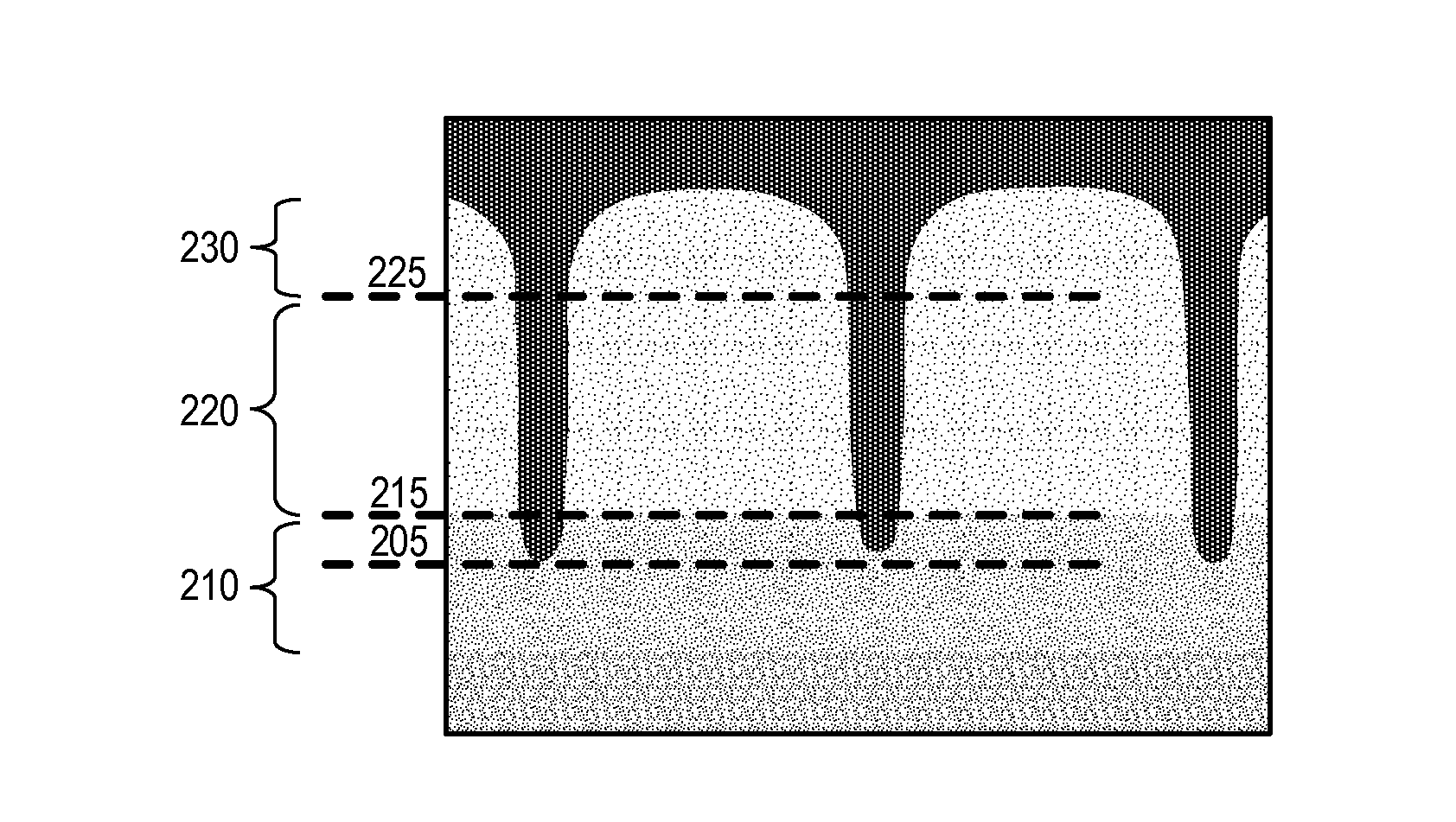
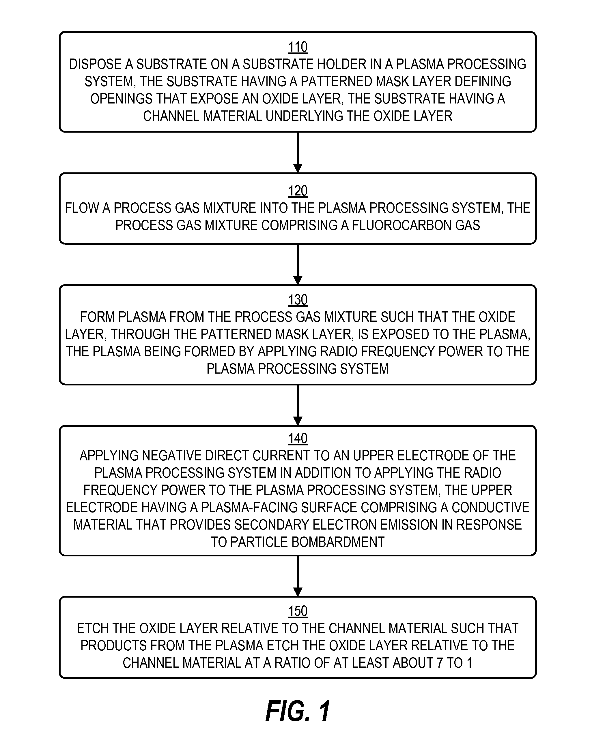
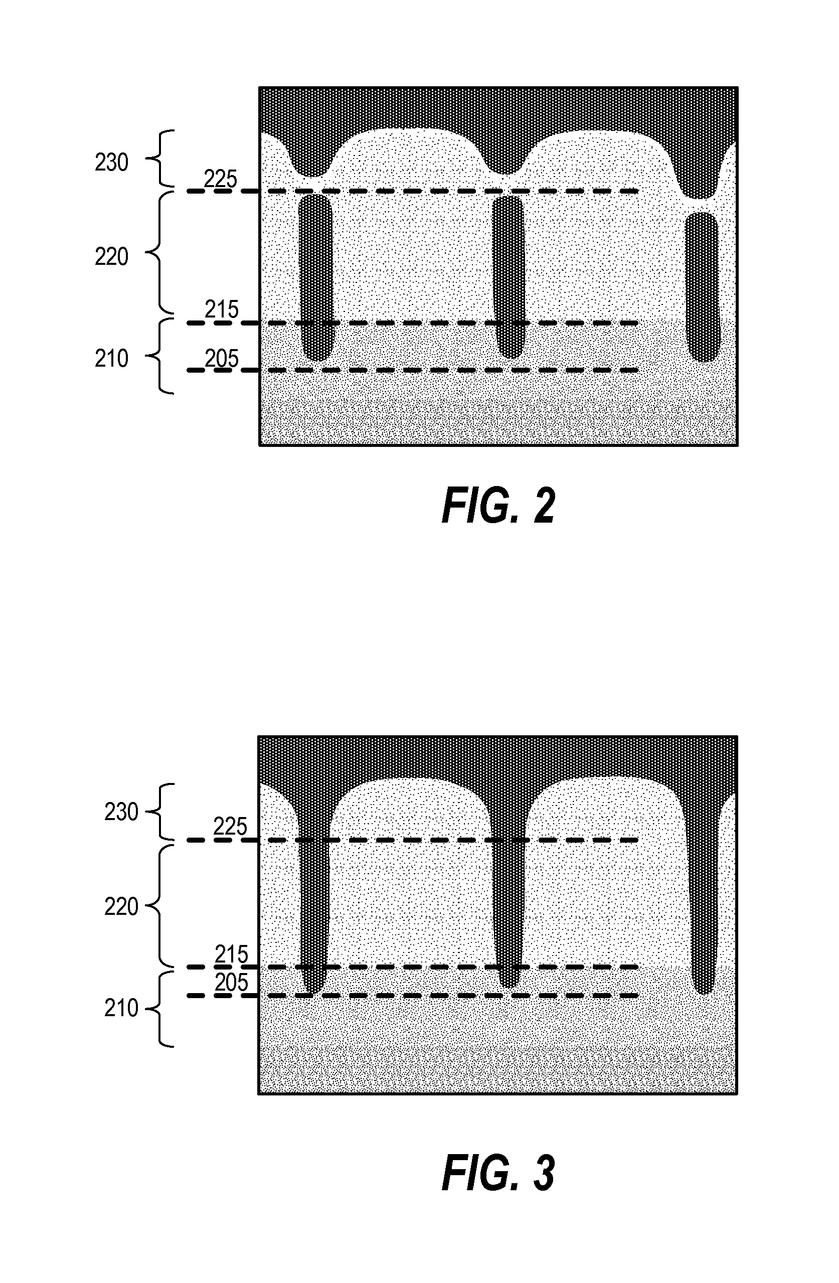
[0013]Techniques herein include methods for etching an oxide layer with greater selectivity to underlying channel materials. Such an increase in etch selectivity reduces damage to channel materials thereby providing more reliable and better performing semiconductor devices. Techniques herein include using fluorocarbon gas to feed a plasma to create etchants, and also creating a flux of ballistic electrons to treat a given substrate during an etch process.

[0014]Techniques herein can be applied to oxide etching and to etching contact-like features through oxide and landing on a source / drain materials. For example, during middle-of-the-line etches, when etching through oxide and landing on silicon germanium (SixGe1-x) there is poor etch selectivity in that a substantial portion of the SiGe is etched. Embodiments can be used for self-aligned contact etch processes, but are not limited to self-aligned contact etching.

[0015]FIG. 1 illustrates a flow chart describing one example embodiment...


PUM


Abstract

Techniques herein include methods for etching an oxide layer with greater selectivity to underlying channel materials. Such an increase in etch selectivity reduces damage to channel materials thereby providing more reliable and better performing semiconductor devices. Techniques herein include using fluorocarbon gas to feed a plasma to create etchants, and also creating a flux of ballistic electrons to treat a given substrate during an etch process.

Description

BACKGROUND OF THE INVENTION[0001]This invention relates to semiconductor processing, and, in particular, to methods and apparatus for etching materials on a substrate.[0002]Various structures and devices are created during the fabrication of logic and memory microchips. For example, transistors, such as field effect transistors, or basic elements of microelectronics and integrated circuits. Fabricating such transistors generally involves depositing layers of various materials, patterning layers, transferring patterns, and removing materials. A common technique for pattern transfer is using a plasma-based etching process, also known as a dry etching process. Such etch-based pattern transfer typically involves a topographic pattern that functions as a mask so that etchants directed toward the substrate etch material in exposed portions of an underlying layer, while the mask prevents etching covered portions of the underlying layer.SUMMARY[0003]In various etch processes, it is common f...

Claims


Application Information

Patent Timeline
IPC IPC(8): H01L21/311
CPCH01L21/31116H01L21/31122H01J37/32091H01J37/32137H01L21/76897H01L21/76802
Inventor METZ, ANDREW
Owner TOKYO ELECTRON LTD
Why Eureka
Try Eureka