Method for Regulating Hardmask Over-Etch for Multi-Patterning Processes

Inactive Publication Date: 2018-05-17
TOKYO ELECTRON LTD
View PDF9 Cites 11 Cited by
  • Summary
  • Abstract
  • Description
  • Claims
  • Application Information

AI Technical Summary

Benefits of technology

The patent text describes a method called SAQP that allows for the creation of smaller patterns in a semiconductor device. The method involves depositing a material called spacer material on a layer, then etching it back to create space between layers. This space is then used as a mask to create the final pattern. The method has advantages such as relaxed pitch and self-aligned patterns. However, the process can be challenging when there are imperfections in the etching. The patent text presents techniques to minimize damage to the underlying layers during the process.

Problems solved by technology

This approach is limited to about 80 nm pitch resolution.
Achieving a smaller pitch is possible, but associated techniques lead to smaller process windows and patterning restrictions (such as used with 1D patterning only).
NA (numerical aperture) 0.33 Extreme Ultraviolet (EUV) lithography can possibly extend pitch resolution to about 24 nm, but EUV tool complexities and costs associated with this technology are too great to be a viable solution.
The spacer etch and etch transfer steps of such multi-patterning can be challenging—especially when material etch resistivities are not perfect.
Imperfect etch resistivities can result in unwanted etching of underlying layers.

Method used


Image

  • Method for Regulating Hardmask Over-Etch for Multi-Patterning Processes
  • Method for Regulating Hardmask Over-Etch for Multi-Patterning Processes
  • Method for Regulating Hardmask Over-Etch for Multi-Patterning Processes

Examples


Embodiment Construction

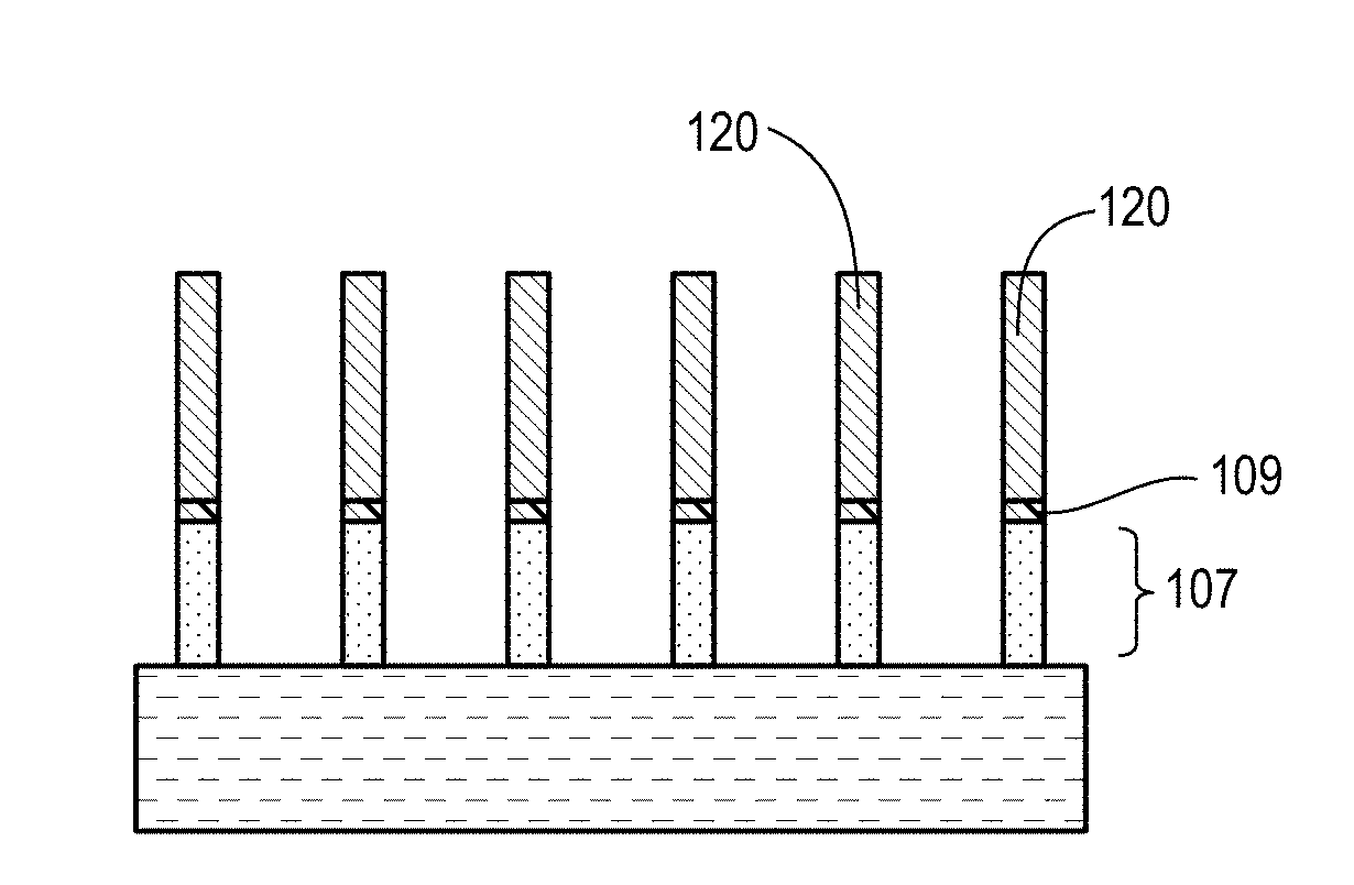
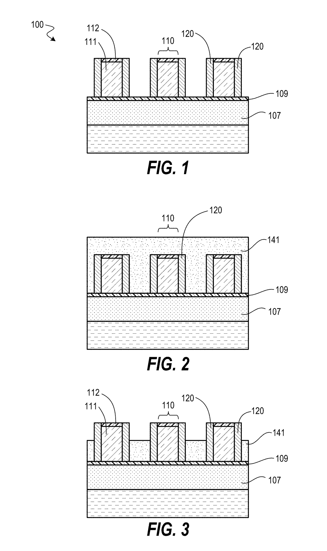
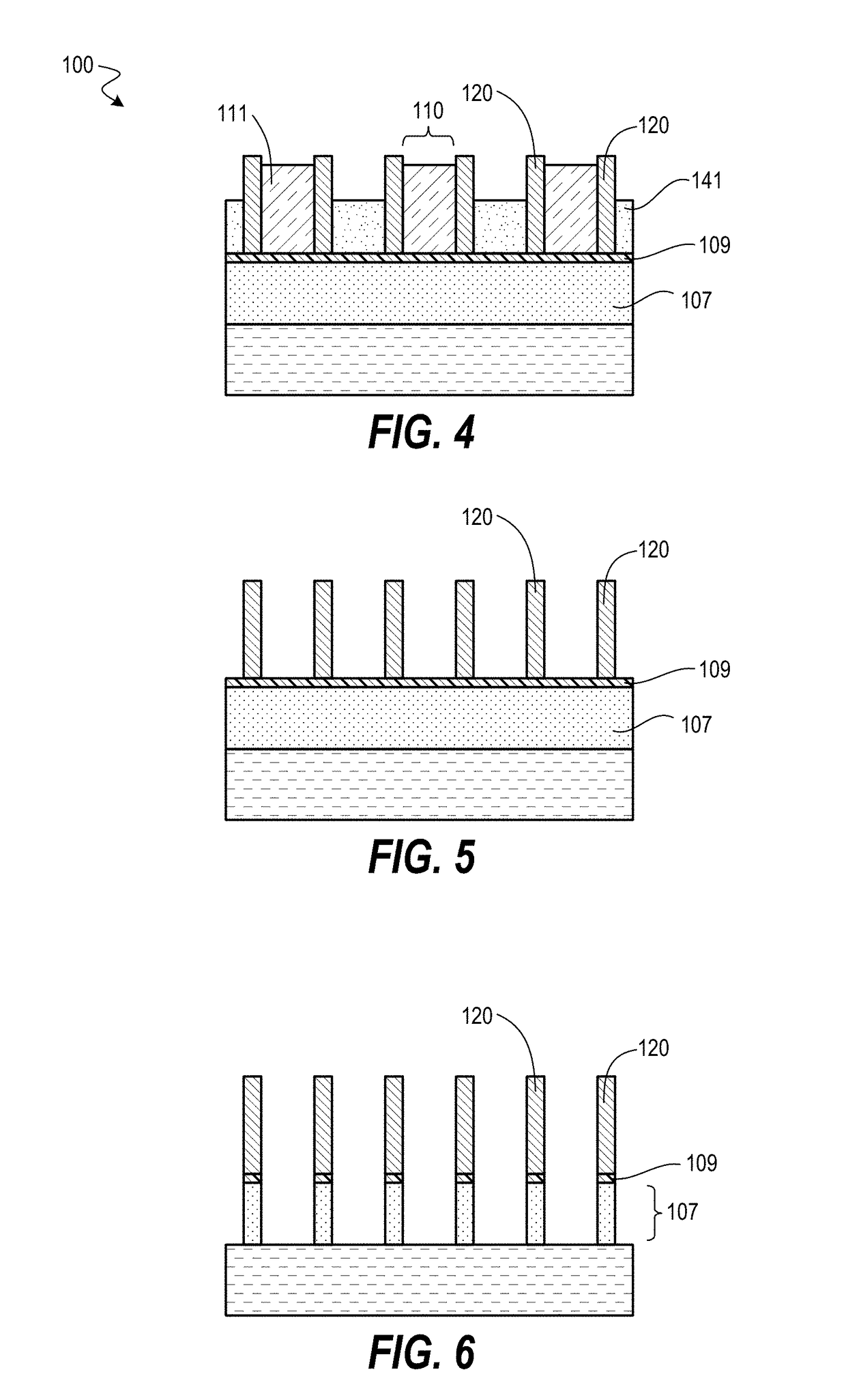
[0021]Techniques herein include patterning processes to prevent over-etching for various multi-patterning processes. Multi-patterning processes typically involve creation of sidewall spacers and removal of mandrels on which sidewall spacers are formed. In some patterning flows gouging of underlying layers can occurs during the various multi-patterning steps. Techniques herein include methods to prevent such gouging by using a planarization layer recessed sufficiently to removed desired materials and protect others. Such techniques can remove bi-layer mandrels without gouging underlying layers.

[0022]SAQP patterning for FEOL (front-end-of-line) applications can be implemented using many different stack and deposition films (amorphous-Silicon, amorphous carbon at 600° C. etc.) because the maximum processing temperature can be approximately 700° C. in some integration schemes. In contrast, when SAQP is used for BEOL (back-end-of-line) applications, the maximum processing temperature is ...


PUM


Abstract

Techniques herein include patterning processes to prevent over-etching for various multi-patterning processes. Multi-patterning processes typically involve creation of sidewall spacers and removal of mandrels on which sidewall spacers are formed. In some patterning flows gouging of underlying layers can occurs during the various multi-patterning steps. Techniques herein include methods to prevent such gouging by using a planarization layer recessed sufficiently to removed desired materials and protect others. Such techniques can remove bi-layer mandrels without gouging underlying layers.

Description

CROSS REFERENCE TO RELATED APPLICATIONS[0001]The present application claims the benefit of U.S. Provisional Patent Application No. 62 / 422,825, filed on Nov. 16, 2016, entitled “Method for Regulating Hardmask Over-etch for multi-patterning processes,” which is incorporated herein by reference in its entirety.BACKGROUND OF THE INVENTION[0002]This disclosure relates to etching features in substrates, including patterning processes for etching substrates.[0003]The fabrication of integrated circuits (IC) in the semiconductor industry typically involves using a plasma reactor to create plasma that assists surface chemistry used to remove material from—and deposit material on—a substrate. Dry plasma etching processes are routinely used to remove or etch material along fine lines or within vias or at contacts patterned on a semiconductor substrate. A successful plasma etching process requires an etching chemistry that includes chemical reactants suitable for selectively etching one material...

Claims


Application Information

Patent Timeline
IPC IPC(8): H01L21/768H01L21/3213
CPCH01L21/7688H01L21/3213B82Y40/00H01L21/31144H01L21/0337H01L21/02107H01L21/02115H01L21/02164H01L21/0217H01L21/022H01L21/0234H01L21/02348H01L21/0332H01L21/0338
Inventor FARRELL, RICHARDMOHANTY, NIHARSMITH, JEFFREY
Owner TOKYO ELECTRON LTD
Why Eureka
Try Eureka