Method for measuring overlay mark and overlay error
A technology of overlay marks and mark patterns, which is applied in the field of semiconductors, can solve the problems that overlay marks are prone to defects, affect the accuracy of overlay error measurement, and reduce product yield, so as to increase the density of patterns and reduce differences , the effect of improving the quality
- Summary
- Abstract
- Description
- Claims
- Application Information
AI Technical Summary
Problems solved by technology
Method used
Image
Examples
Embodiment Construction
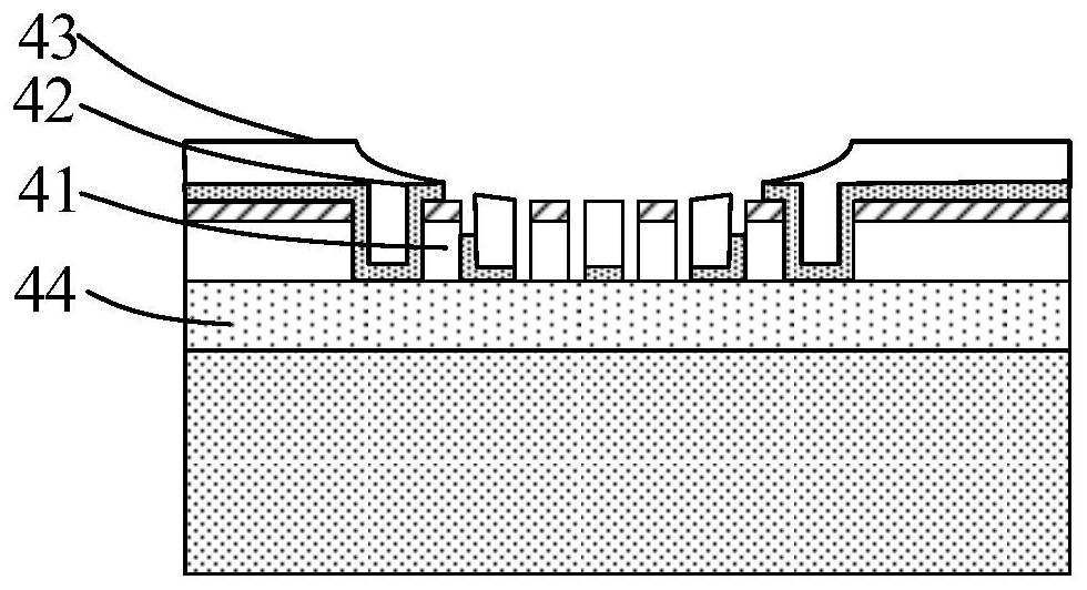
[0024] It can be seen from the background art that the overlay marks are prone to defects during the formation process. The analysis found that the main reason is that the overlay marks belong to the low-density pattern area relative to the array area. Based on the etching load effect, the reactive ions in the pattern-intensive area are The active ingredients are consumed quickly, and the etching rate is reduced; on the contrary, the etching rate of the pattern sparse area is higher, resulting in the problems of over-etching and different degrees of etching.
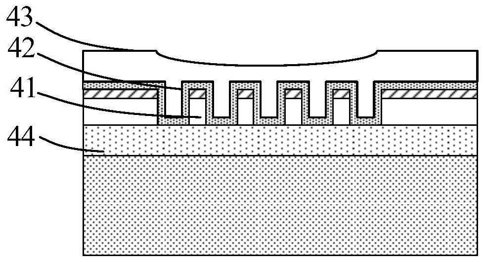
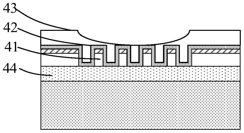
[0025] For example, Figure 1-Figure 4 A schematic diagram of the structure corresponding to each step in a method for manufacturing an overlay mark is shown. Specifically, refer to figure 1 , a spin-coatable dielectric layer 43 is coated on the first mask layer 41 and the second mask layer 42 . refer to figure 2 , the spin-coatable dielectric layer 43 is etched back to expose the top surface of the second mask layer ...
PUM
 Abstract
Description
Claims
Application Information


