
Novel process for improved hot carrier injection

An injection effect and carrier technology, which is applied in the manufacture of electrical components, electrical solid devices, semiconductor/solid devices, etc., can solve problems such as poor process pass rate, shortened hot carrier degradation time, and slipping of component electrical stability

Active Publication Date: 2005-07-13
TAIWAN SEMICON MFG CO LTD
View PDF0 Cites 4 Cited by
  • Summary
  • Abstract
  • Description
  • Claims
  • Application Information

AI Technical Summary

Problems solved by technology

The effect of such charge accumulation cannot be eliminated by additional steps of tempering (Anneal)
As a result, the plasma charge accumulated in the component will lead to a more serious hot carrier injection effect, and the hot carrier degradation time of the component will be greatly shortened
As a result, the electrical stability of the components will drop significantly, resulting in a significant drop in the reliability of the components and a poor process pass rate

Method used


Image

  • Novel process for improved hot carrier injection
  • Novel process for improved hot carrier injection

Examples


Embodiment Construction

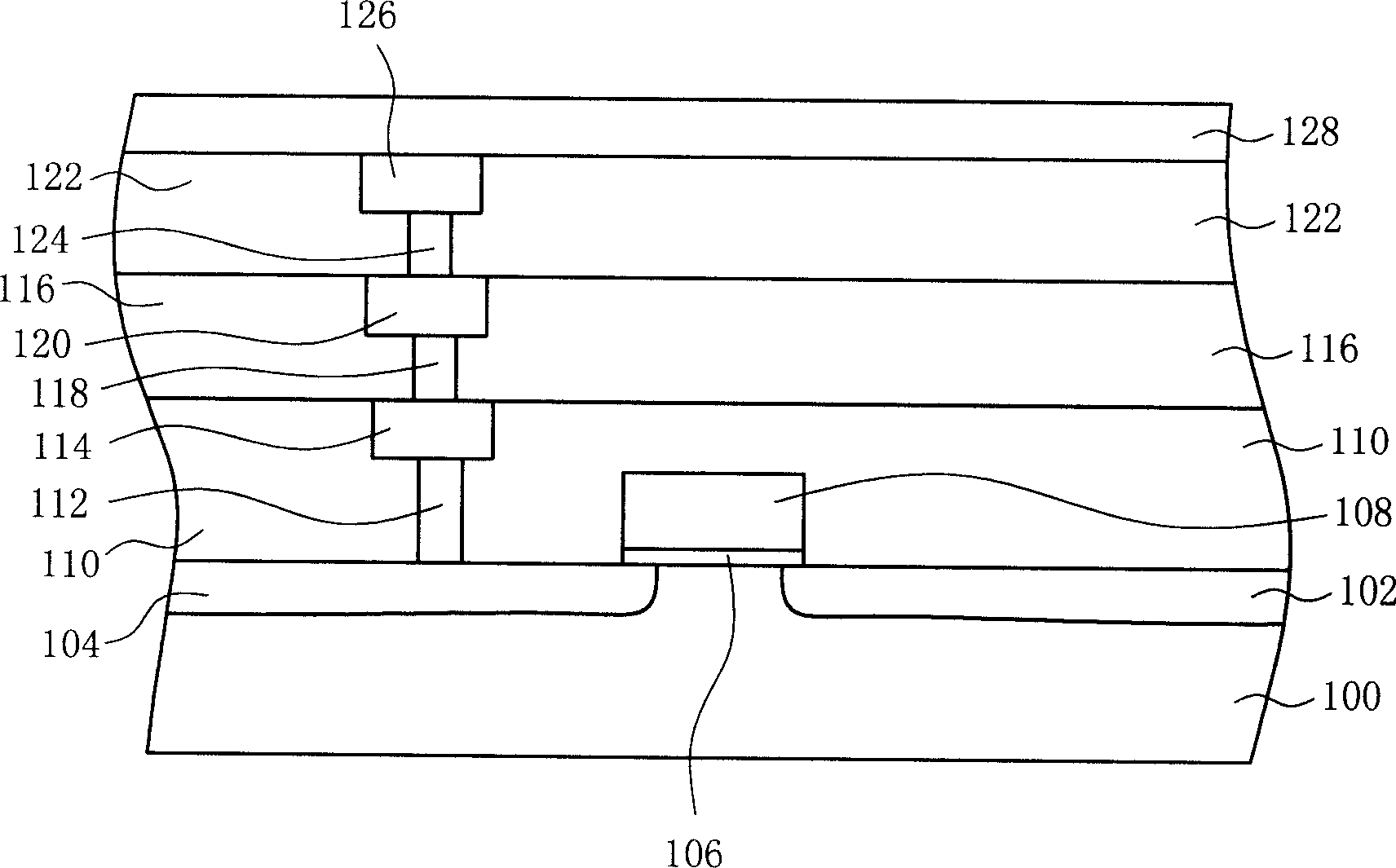
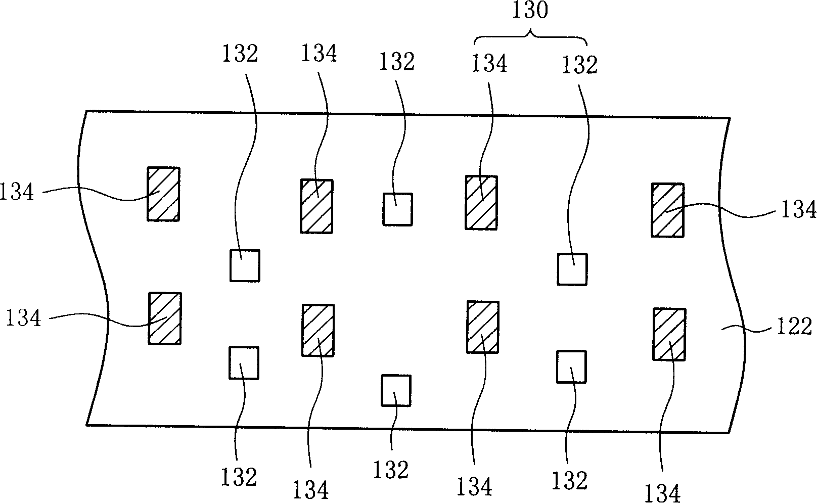
[0043]The invention discloses a method for improving the hot carrier injection effect, and shortens the plasma etching time by increasing the pattern density of the aluminum welding pad. Therefore, the damage of the plasma to the element can be reduced, and the hot carrier injection effect of the element can be improved, thereby achieving the purpose of improving the electrical reliability of the element. In order to make the narration of the present invention more detailed and complete, refer to the following description and cooperate figure 1 and figure 2 .

[0044] Please refer to figure 1 , figure 1 A cross-sectional view of an element structure according to a preferred embodiment of the present invention is shown. The method for improving the hot carrier injection effect of the present invention firstly provides a semiconductor substrate 100 . A thin gate dielectric layer 106 is then formed on the surface of the substrate 100 by means such as rapid thermal oxidation...


PUM


Abstract

A method for improving hot carrier injection effect (Hot Carrier Injection Effect; HCI Effect), including the steps of: providing a substrate; and forming a soldering pad layer located on part of the substrate, wherein the soldering pad layer includes the required There are a plurality of circuit patterns and a plurality of dummy patterns (Dummy Patterns), and the pad layer has a pattern density. In this method, in the semiconductor copper process, multiple dummy patterns (Dummy Patterns) are set when etching the aluminum pad (AlPad) to shorten the etching time of the aluminum pad. Therefore, the damage caused by the etching plasma to the component can be reduced, thereby prolonging the degradation time of hot carrier injection of the component.

Description

technical field [0001] The present invention relates to a method for improving the hot carrier injection effect (Hot Carrier Injection Effect; HCIE Effect), in particular to a method of shortening the etching time of the aluminum pad by increasing the pattern density of the aluminum pad (Al Pad) to improve the heat load method of sub-injection effects. Background technique [0002] In the semiconductor process, when the electrons are in the electric field, the electrons will be accelerated due to the attraction of the positive potential and gain kinetic energy. The electrons with high kinetic energy are called hot carriers. For example, when the channel length of a MOS Transistor is shortened, if the applied voltage remains constant, the lateral electric field in the channel will increase. In this way, after the electrons in the channel are accelerated by the electric field, the energy of the electrons is greatly increased. Because the electrons accelerated by the electric...

Claims


Application Information

Patent Timeline
Patent Type & Authority Applications(China)
IPC IPC(8): H01L21/28H01L21/302H01L21/311H01L21/3205H01L21/3213H01L21/461H01L21/60H01L21/768H01L23/485
CPCH01L21/32136H01L21/32139H01L24/03H01L24/05H01L2224/05624H01L2924/01013H01L2924/01014H01L2924/01029H01L2924/01082H01L2924/14H01L2924/19043H01L2924/01033H01L2924/13091H01L2224/06517H01L2924/00014H01L2924/00
Inventor 简财源忻斌一
Owner TAIWAN SEMICON MFG CO LTD
Learn More