Organic light emitting diode device

Inactive Publication Date: 2011-08-18
KOREA ADVANCED INST OF SCI & TECH
View PDF5 Cites 7 Cited by
  • Summary
  • Abstract
  • Description
  • Claims
  • Application Information

AI Technical Summary

Benefits of technology

[0011]Accordingly, the present invention has been made to solve the above-mentioned problems, and an object of the present invention is to provide an organic light emitting diode (OLED) device which can improve current char

Problems solved by technology

In this case, when the difference in energy level between the cathode and anode of the OLED device and the organic EL element layer is large, a high energy barrier is formed at the time of carrier injection, and thus a large amount of power is consumed during the procedure of actually outpu

Method used


Image

  • Organic light emitting diode device
  • Organic light emitting diode device
  • Organic light emitting diode device

Examples


Embodiment Construction

[0047]The above and other objects, features and advantages of the present invention will be more clearly understood from the following detailed description taken in conjunction with the accompanying drawings.

[0048]Hereinafter, preferred embodiments of the present invention will be described in detail with reference to the attached drawings. Here, the detailed description of commonly-known constitutions and functions related to the present invention will be omitted.

[0049]Hereinafter, an organic light emitting diode device according to an embodiment of the present invention will be described in detail with reference to FIGS. 2 to 20.

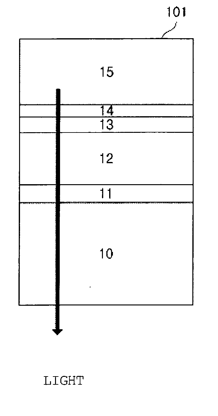
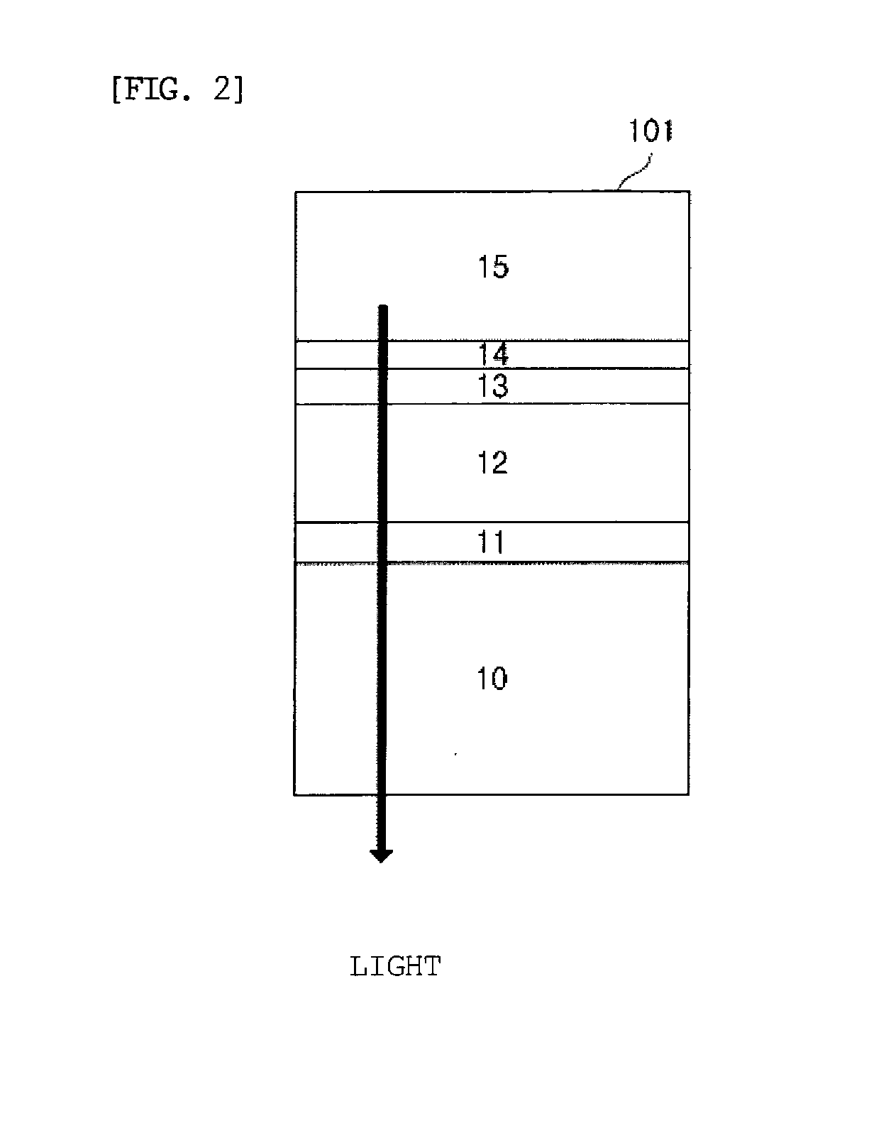
[0050]FIG. 2 is a schematic view showing an organic light emitting diode (OLED) device according to an embodiment of the present invention.

[0051]Referring to FIG. 2, the OLED device 101 includes a substrate 10, a lower electrode layer 11, organic EL element layers 12 and 13, a metal nanocluster layer 14, and an upper electrode layer 15.

[0052]The lower elec...


PUM


Abstract

Disclosed herein is an organic light emitting diode device, including: an organic EL element layer; an electrode layer supplying power to the organic EL element layer; and a metal nanocluster layer which is formed by covering a plurality of metal clusters with media and which is located between the organic EL element layer and the electrode layer to induce a luminescence enhancement effect. The organic light emitting diode device is advantageous in that carriers can be easily injected, so that light output efficacy is improved, thereby enhancing fluorescent emission output.

Description

BACKGROUND OF THE INVENTION[0001]1. Technical Field[0002]The present invention relates to an organic light emitting diode (OLED) device, and, more particularly, to an organic light emitting diode (OLED) device which can improve carrier injection and fluorescence emission effects using metal nanoclusters.[0003]2. Description of the Related Art[0004]An organic light emitting diode (OLED) device, which is a device producing luminescence by the reaction occurring when a voltage is applied, was described in the paper ‘Applied Physics Letters. 51, 913 (1987)’, written by C. W. Tang, S. A. VanSlyke et al. and U.S. Pat. No. 4,769,292. Thereafter, a plurality of organic electroluminescent (EL) element layers were proposed, thus improving the performance of OLED devices.[0005]As shown in FIG. 1, a general OLED device 100 includes a substrate 10, a lower electrode layer 11, organic EL element layers 12 and 13, and an upper electrode layer 15. The organic EL element layers 12 and 13 include one...

Claims


Application Information

Patent Timeline
IPC IPC(8): H01L33/58H01L33/60
CPCB82Y20/00H01L2251/5369H01L51/5092B82Y30/00H10K50/171H10K2102/331H01L21/26566H10K50/15H10K50/16H10K50/11
Inventor CHOI, KYUNG CHEOLYANG, KI YOUL
Owner KOREA ADVANCED INST OF SCI & TECH
Why Eureka
Try Eureka