Modulated multi-frequency processing method

a multi-frequency processing and modulated technology, applied in plasma etching, electric discharge tubes, light sources, etc., can solve the problems of reducing feature charging, etching such narrow and deep features, and reducing feature charging, so as to reduce the dispersion of etched contact holes, reduce the selectivity of contact to mask etching, and reduce the polymerizing properties of the process.

Active Publication Date: 2010-10-07
LAM RES CORP
View PDF10 Cites 3 Cited by
  • Summary
  • Abstract
  • Description
  • Claims
  • Application Information

AI Technical Summary

Benefits of technology

[0020]In the conventional HARC etch process, the distortion of etched contact holes can be minimized by reducing the power of the continuous high frequency portion of the signal provided by RF driver 110. However, this method decreases the polymerizing properties of the process and therefore decreases contact-to-mask etch selectivity. Also, this method decreases the plasma density and ion flux, thereby slowing down the etch rate.

Problems solved by technology

The etching of such narrow and deep features poses many challenges due to various complications and difficulties that arise during the plasma etching process.
First, they may reduce feature charging during an etching process by discharging sidewalls.
Second, low energy ions may contribute to polymer deposition during an etching process to protect a mask.
Additionally, a relatively large power of the continuous high frequency portion of the driving signal will typically increase distortion of the etched hole, as will be discussed below with reference to FIG. 5A.
However, this method decreases the polymerizing properties of the process and therefore decreases contact-to-mask etch selectivity.
Also, this method decreases the plasma density and ion flux, thereby slowing down the etch rate.

Method used


Image

  • Modulated multi-frequency processing method
  • Modulated multi-frequency processing method
  • Modulated multi-frequency processing method

Examples


Embodiment Construction

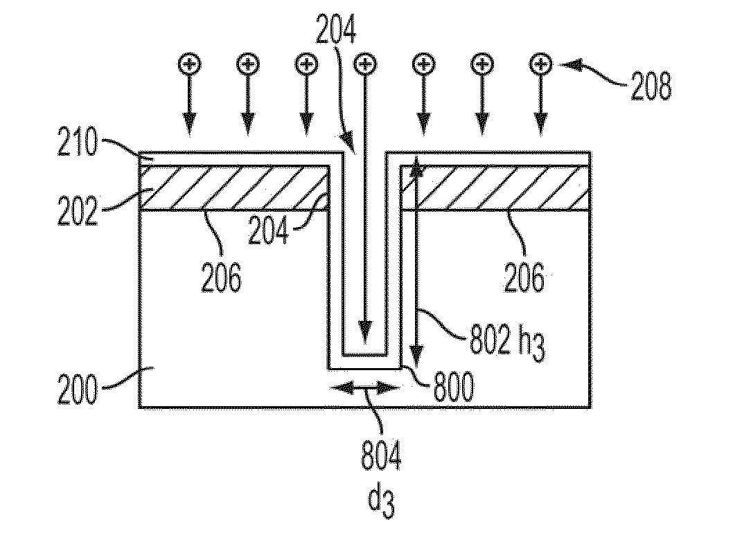
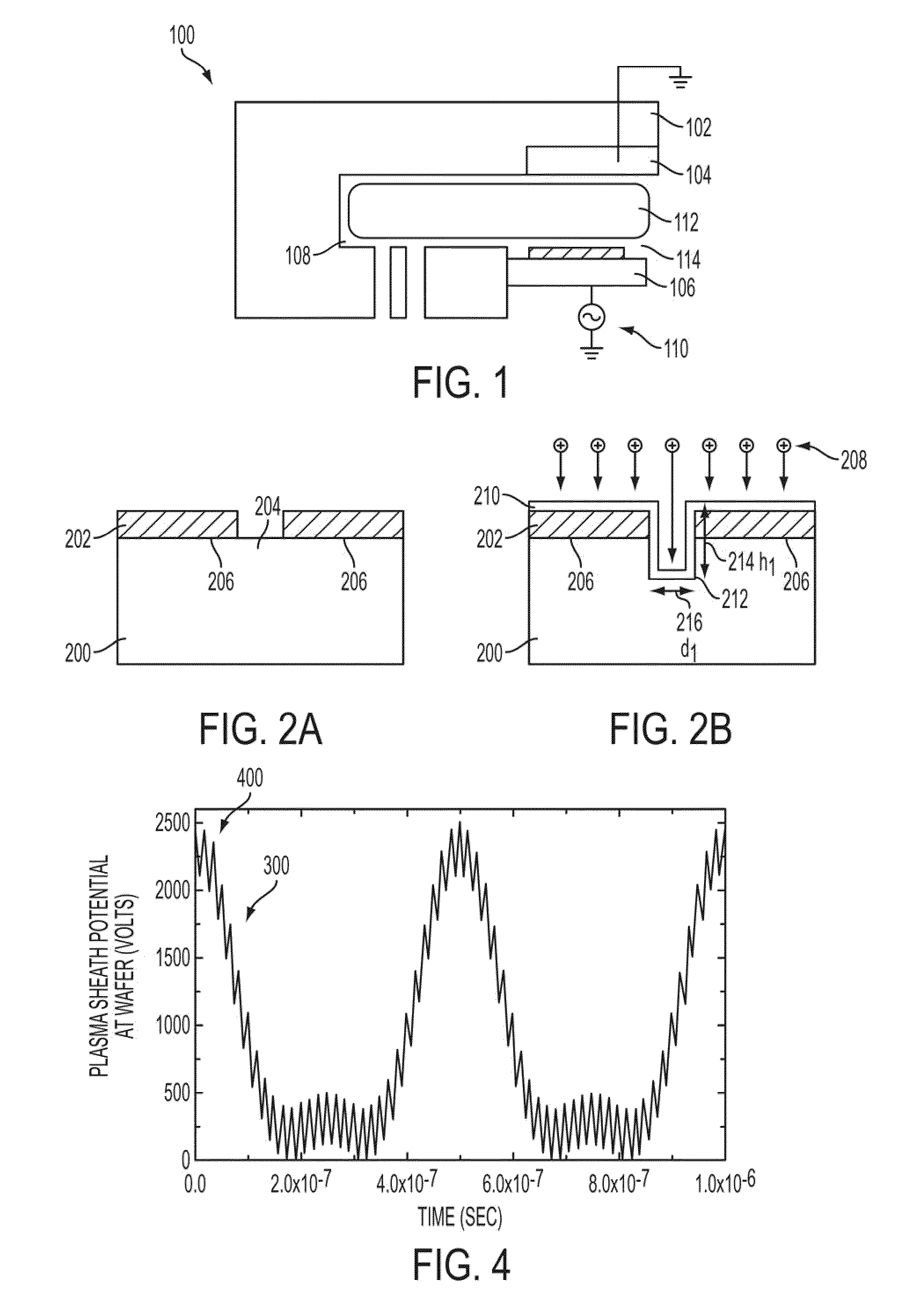
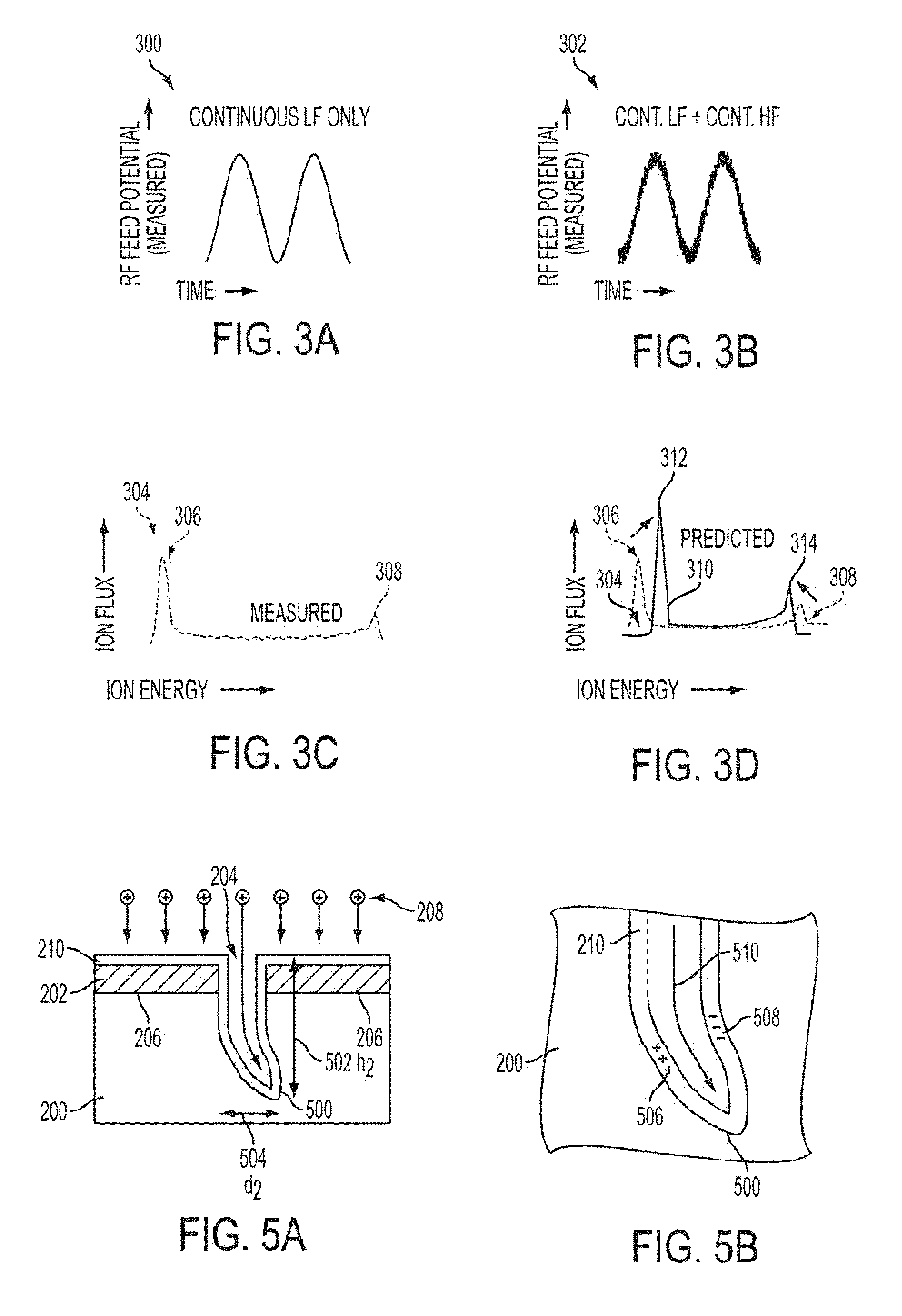
[0043]In accordance with an aspect of the present invention, a system and method provides for best HARC etch with no contact hole distortion, while maintaining a high etch rate for high throughput. More particularly, in accordance with an aspect of the present invention, a processing system that is operable to generate a plasma by way affecting a gas with an electromagnetic field, is operated in a particular manner to control a parameter as a function of time that is based on a low frequency sinusoidal portion and a high frequency sinusoidal portion. The high frequency sinusoidal portion is amplitude-modulated at a frequency equal to a harmonic of the low frequency sinusoidal portion. Further, the high frequency sinusoidal portion includes a high amplitude interval and a low amplitude interval. The duration of the duty cycle of the high frequency sinusoidal portion is the ratio of the duration of the high amplitude interval to the sum of the duration of the high amplitude interval a...


PUM


Abstract

A method is provided for operating a processing system having a space therein arranged to receive a gas and an electromagnetic field generating portion operable to generate an electromagnetic field within the space. The method includes providing a gas into the space, and operating the electromagnetic field generating portion with a driving potential to generate an electromagnetic field within the space to transform at least a portion of the gas into plasma. The driving potential as a function of time is based on a first potential function portion and a second potential function portion. The first potential function portion comprises a first continuous periodic portion having a first amplitude and a first frequency. The second potential function portion comprises a second periodic portion having an maximum amplitude portion, and minimum amplitude portion and a duty cycle. The maximum amplitude portion is a higher amplitude than the minimum amplitude portion. The duty cycle is the ratio of a duration of the maximum amplitude portion to the sum of the duration of the maximum amplitude portion and the duration of the minimum amplitude portion. The second periodic portion additionally has a second frequency during the maximum amplitude portion. An amplitude modulation of the second periodic portion is phase locked to the first continuous periodic portion.

Description

[0001]The present application claims priority from U.S. Provisional Application No. 61 / 166,987 filed Apr. 6, 2009, the entire disclosure of which is incorporated herein by reference.BACKGROUND[0002]In the semiconductor manufacturing industry, plasma etching is widely used in wafer processing. It is typically used to create features such as contact holes or trenches in materials in order to form electrical contacts. Given that space is an important consideration in manufacturing, it is often desirable to make these contact holes as narrow and as deep as possible. The etching of such narrow and deep features poses many challenges due to various complications and difficulties that arise during the plasma etching process.[0003]FIG. 1 illustrates a cross-sectional view of a left side of a conventional wafer processing system during a conventional plasma etching process. Wafer processing system 100 includes a processing chamber 102, an upper electrode 104; an electro-static chuck (ESC) 10...

Claims


Application Information

Patent Timeline
Patent Type & Authority Applications(United States)
IPC IPC(8): H05B31/26
CPCH01J37/32009H01J37/32137H01L21/3065H01J2237/3348H01J2237/334H01J37/32146H01L21/02H01L21/205H01L21/76825H01L21/76826H05H1/24H05H1/36
Inventor MARAKHTANOV, ALEXEIHUDSON, ERICDHINDSA, RAJHINDERBAILEY, III, ANDREW D.
Owner LAM RES CORP
Why Eureka
Try Eureka