
Interface device and control method thereof

Active Publication Date: 2018-09-27
CANON KK
View PDF0 Cites 3 Cited by
  • Summary
  • Abstract
  • Description
  • Claims
  • Application Information

AI Technical Summary

Benefits of technology

The invention helps control how different parts of a computer access and use memory, so that they can communicate data with each other more efficiently.

Problems solved by technology

Hence, as a result, DRAM page misses, bank conflicts, and read / write switching frequently occur, and the memory access latency becomes very long.
This ultimately results in the degradation of the performance of the embedded device.
Hence, as these modules have a small memory access unit (transfer length) for each memory access, it is difficult to sufficiently bring out the performance of the latest external memory (DRAM) standard.
Also, since no measures are taken against the high memory-access latency in a reused image processing module, the performance will degrade instead.
Also, when many memory accesses are caused by many uncontrolled data processing circuits (masters), access conflicts to the DRAM occur frequently, and DRAM page misses, read / write switching, and bank conflicts occur.
Thus, the latency of one memory access operation becomes very high.
Since the above-described conventional techniques do not consider a case in which very many data processing circuits (master) are not controlled and perform memory accesses to the DRAM, performance degradation occurs.
Also, the above-described conventional techniques do not disclose any measures for a form using a next-generation DRAM, a form in which a plurality of semiconductor chips are connected to each other, and a form in which many sensors are connected to a semiconductor chip.
Furthermore, the above-described conventional techniques do not disclose any measures for reused image processing modules (data processing circuits), for a case in which new and old sensors with different specifications are present, and for a case in which sensor specifications are changed.

Method used


Image

  • Interface device and control method thereof
  • Interface device and control method thereof
  • Interface device and control method thereof

Examples


first embodiment

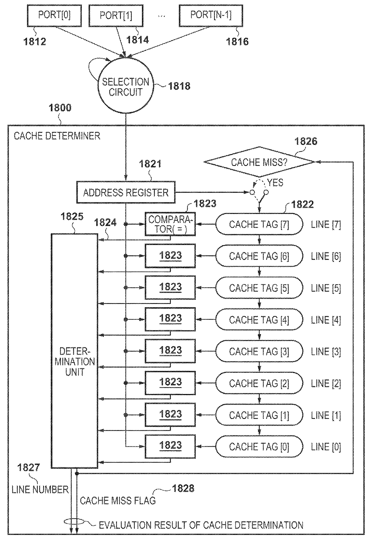
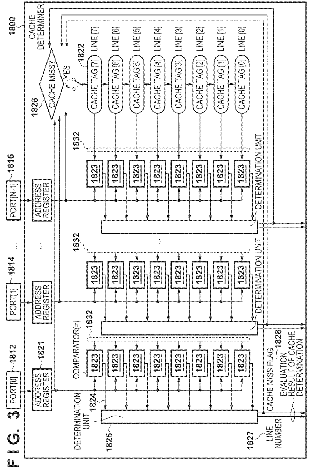
[0029]An example of a multiport shared cache incorporated in an information processing apparatus will be raised as an interface device of the first embodiment according to the present invention.

[0030]

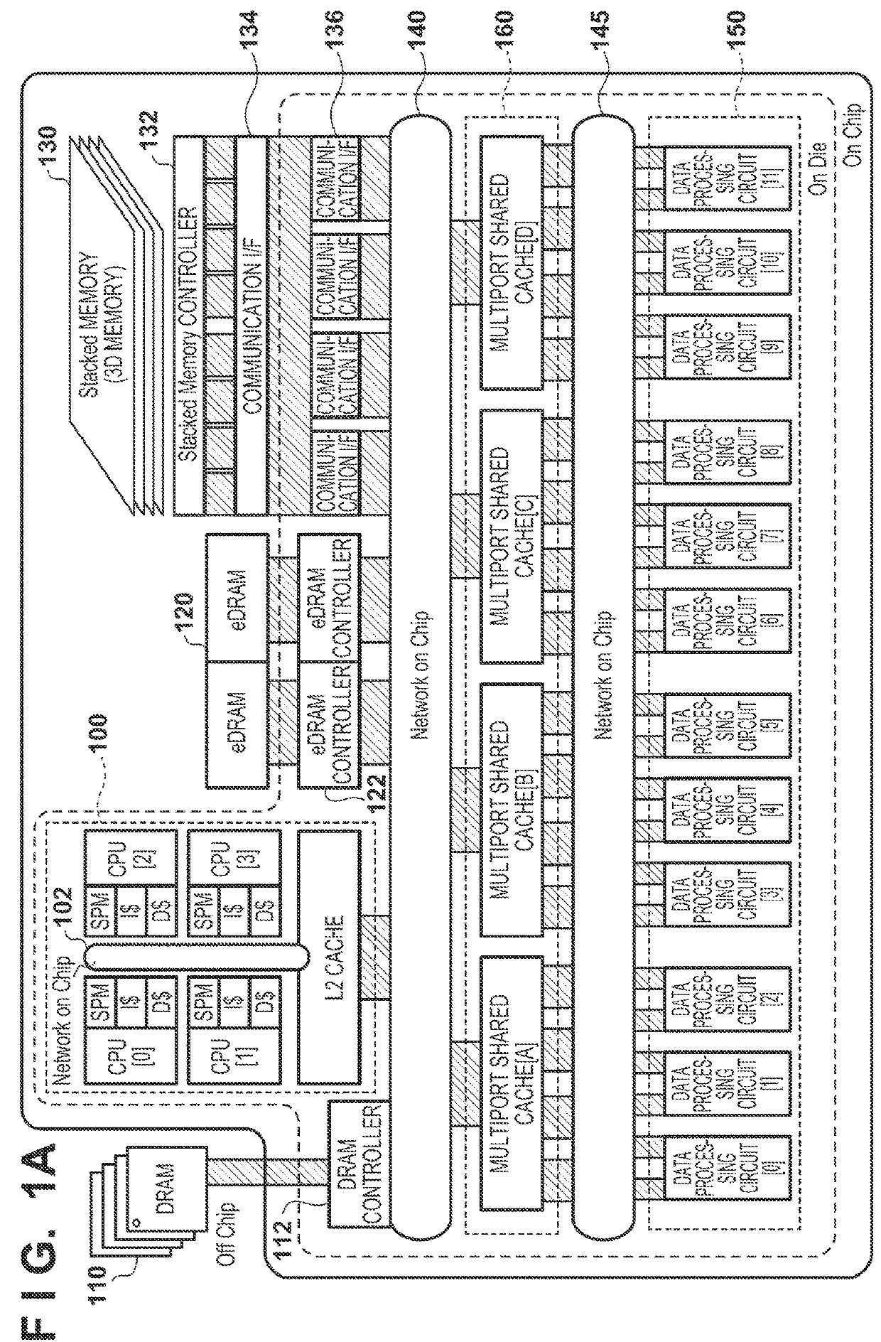
[0031]FIG. 1A is a block diagram showing the arrangement of the information processing apparatus according to the first embodiment. More specifically, FIG. 1A shows an information processing apparatus to which a multiport shared cache formed to be capable of accepting data requests via N ports has been inserted.

[0032]The information processing apparatus includes a CPU circuit unit 100, external memories, an image processing unit 150, and the multiport shared cache 160. A DRAM 110, an eDRAM (embedded DRAM or mixed DRAM) 120, and a stacked memory (three-dimensional memory) 130 are examples of external memories. The information processing apparatus also includes a system bus (Network On Chip / shared bus) 140, an image processing bus (Network On Chip / shared bus) 145, and the like.

[0033]The C...

second embodiment

[0191]In the first embodiment described above, the DRAM 110, the eDRAM 120, the stacked memory 130, or the like was set as the external memory to describe a memory access method from a multiport shared cache.

[0192]In the second embodiment, a DRAM 110 and a stacked memory 130 are set as the external memories. Each eDRAM 120 is set as cache memories [0] to [N−1], and cache memory controllers [0] to [N−1] are connected to inputs and outputs of a corresponding eDRAM controller 122. Also, in this embodiment, data acquirers fetch [0] to fetch [N−1] including cache memories [0] to [4N−1] and cache memory controls [0] to [4N−1] are incorporated in the stacked memory 130.

[0193]As in the above-described FIGS. 6A and 6B, for the multiport shared cache, a prefetch unit 410 and a fetch unit 430 are loosely coupled by a command intermediate FIFO. Hence, in the manner of embodiment, the prefetch unit 410 is inserted in the insertion position of the multiport shared cache according to the first emb...

third embodiment

[0201]An interface form between chips each including a multiport shared cache will be described in the third embodiment.

[0202]Conventionally, when image data that has been processed by an image processing unit 720 of a chip A is to be processed in an image processing unit 730 of a chip B, a CPU (not shown) controls a transfer DMAC (not shown) to transfer the image data from a DRAM 710 to a DRAM 712. Hence, the CPU needs to control the aforementioned DMAC to transfer large units of image data during the processing completions of respective image processors (data processing circuits) [0] to [7]. Since the number of DMACs increases as the number of image processing units (data processing circuits) is increased, DMAC control by the CPU becomes very complex, and the image processing throughput may be affected.

[0203]

[0204]FIG. 14 is a block diagram showing the arrangement of an information processing apparatus according to the third embodiment. Here, multiport shared caches are used to im...


PUM


Abstract

In order to allow efficient data communication, an interface device that includes N ports, comprises: a cache memory that is shared by the N ports and includes a plurality of cache tags each of which is allocated to one of the N ports; and N cache determination units corresponding to the N ports. Each of the N cache determination units comprises: a determiner configured to determine, based on all of the values of the plurality of cache tags, whether a cache miss has occurred in the cache memory, and an update unit configured to update, when the determiner determines that a cache miss has occurred, cache tag values allocated to a self-port.

Description

BACKGROUND OF THE INVENTIONField of the Invention[0001]The present invention relates to a data communication technique.Description of the Related Art[0002]In recent years, due to increased miniaturization of semiconductor processes, even semiconductor chips for embedded devices have undergone large-scale integration, and very many masters are present in a chip. Since many masters read / write data from / in an external memory (DRAM or the like), accesses to the external memory concentrate. As a result, continuous accesses to an external memory will lead to accesses to different DRAM pages and banks, and this increases random accessibility. Hence, as a result, DRAM page misses, bank conflicts, and read / write switching frequently occur, and the memory access latency becomes very long. This ultimately results in the degradation of the performance of the embedded device.[0003]On the other hand, in the specification development of a DRAM, which is a storage device generally used as an extern...

Claims


Application Information

Patent Timeline
IPC IPC(8): G06F12/0815G06F12/0855
CPCG06F12/0815G06F12/0855G06F2212/1008G06F2212/1021G06F12/084G06F12/0846G06F12/0853
Inventor ITO, TADAYUKI
Owner CANON KK
Features
  • Generate Ideas
  • Intellectual Property
  • Life Sciences
  • Materials
  • Tech Scout
  • Unparalleled Data Quality
  • Higher Quality Content
  • 60% Fewer Hallucinations
Learn More