Self-assembly of perovskite for fabrication of transparent devices

a technology of perovskite and transparent devices, which is applied in the direction of light-sensitive devices, solid-state devices, and electrolytic capacitors, etc., can solve the problems of high capital investment, difficult to precisely control the transparency of the cell, and high cost of evaporation-based processes, so as to reduce or diminish the recombination process, improve the surface area, and excellent reliability and durability features

Active Publication Date: 2018-09-27
YISSUM RES DEV CO OF THE HEBREWUNIVERSITY OF JERUSALEM LTD
View PDF3 Cites 12 Cited by
  • Summary
  • Abstract
  • Description
  • Claims
  • Application Information

AI Technical Summary

Benefits of technology

[0010]The use of this method not only established means to direct the perovskite material to be formed on the walls of the screen, defining precisely a desired pattern and therefore endowing the ability to control certain features of the pattern (e.g., the openings size or the thickness of the perovskite rim or side, leading to control of the pattern transparency and conductivity), but also insured fabrication of continuous patterns having uniform composition throughout the film, and endowing the ability to form large-scale patterns with excellent reliability and durability features (of the device based thereon). Thus, the present invention is aimed at providing novel (transparent) continuous perovskite patterns, processes for their production and uses thereof in the construction of photo / electronic devices (e.g., semitransparent solar cell).
[0316]In some embodiments, the at least one scaffold comprises a metal oxide, wherein the at least one scaffold pattern (substantially) increases the effective surface area of the substrate, and optionally the at least one scaffold layer is present between the substrate and the perovskite layer.

Problems solved by technology

Moreover, it seems that with this method it is difficult to precisely control the transparency of the cell.
However, evaporation-based processes are very costly, require high capital investments, and are very complicated for up-scaling, which is required for industrial applications.
In addition, the evaporation technique, using only a thin film of the absorber material in the solar cell (i.e. the perovskite) leads to a decrease of the overall solar cell efficiency.

Method used


Image

  • Self-assembly of perovskite for fabrication of transparent devices
  • Self-assembly of perovskite for fabrication of transparent devices
  • Self-assembly of perovskite for fabrication of transparent devices

Examples


Embodiment Construction

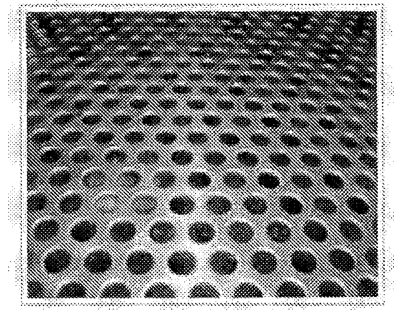
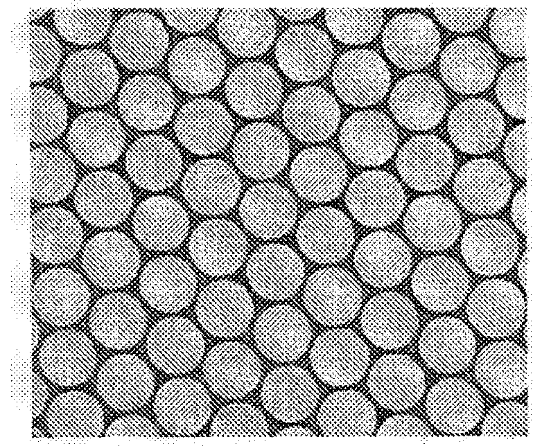
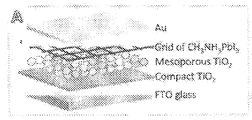
[0374]This work reports on semi-transparent hole conductor free perovskite solar cells. The cells transparency is achieved through a unique wet deposition technique that creates perovskite grids with various dimensions. The perovskite grid is deposited on a mesoporous TiO2 layer, followed by evaporation of semi-transparent gold film. No hole conductor is used in this solar cell structure; however a hole conductor may be used in other embodiments of the solar cell. Control of the transparency of the solar cells is achieved by changing the perovskite solution concentration and the mesh openings. The semi-transparent cells demonstrate 20%-70% transparency. This is the first demonstration of the possibility to create a perovskite pattern using self-assembly deposition method for fabrication of a semitransparent perovskite based solar cell.

[0375]Here we report on a unique, simple wet deposition method for the fabrication of semi-transparent perovskite-based solar cells. This deposition m...


PUM

PropertyMeasurementUnit
transparentaaaaaaaaaa
diameteraaaaaaaaaa
diameteraaaaaaaaaa

Abstract

Provided is a continuous material pattern, the pattern is selected to have a plurality of material-free voids, the material including at least one perovskite material.

Description

TECHNOLOGICAL FIELD[0001]The invention disclosed herein generally relates to the construction of novel semi-transparent or transparent perovskite-based electronic or optoelectronic devices (e.g., solar cells) and novel hybrid meso-planar perovskite-based electronic or optoelectronic devices.BACKGROUND[0002]An attractive application of semi-transparent photovoltaic (PV) solar cells is the possibility to use them in building integrated elements that can lead to self-sustaining buildings at low cost. Organic and inorganic materials have been widely used for the development of semi-transparent solar cells and have been suggested for integration in office buildings and replacement windows. This integration offers harvesting of solar energy over wider surfaces.[0003]Thus far, there are only a few reports about the development of semi-transparent perovskite solar cells. Eperon et al [1] used a strategy which relied on de-wetting of a perovskite film to create ‘perovskite islands’; thus ach...

Claims


Application Information

Patent Timeline
Patent Type & Authority Applications(United States)
IPC IPC(8): H01G9/20H01L51/42H01L51/00
CPCH01G9/2009H01L51/0077H01G9/2045H01L51/4213H01L51/4226H10K30/151H10K30/10Y02E10/549Y02E10/542H10K85/00H10K85/50H10K85/30
Inventor ETGAR, LIOZMAGDASSI, SHLOMOAHARON, SIGALITLAYANI, MICHAEL
Owner YISSUM RES DEV CO OF THE HEBREWUNIVERSITY OF JERUSALEM LTD
Why Eureka
Try Eureka