Method of forming semiconductor device

a semiconductor and device technology, applied in the field of semiconductor devices, can solve the problems that the current planar fets no longer meet the requirements of products, and achieve the effect of good lattice structur

Active Publication Date: 2018-10-25
UNITED MICROELECTRONICS CORP
View PDF7 Cites 6 Cited by
  • Summary
  • Abstract
  • Description
  • Claims
  • Application Information

AI Technical Summary

Benefits of technology

[0008]Based on the semiconductor device and the method set forth in the present invention, which is characterized by using the semiconductor layer as a buffer layer, the formed fin structures can have good lattice structure and no fin cut process is required.

Problems solved by technology

However, with the increasing miniaturization of electronic products, current planar FETs no longer meet the requirements of the products.

Method used


Image

  • Method of forming semiconductor device
  • Method of forming semiconductor device
  • Method of forming semiconductor device

Examples


Embodiment Construction

[0014]To provide a better understanding of the presented invention, preferred embodiments will be made in detail. The preferred embodiments of the present invention are illustrated in the accompanying drawings with numbered elements.

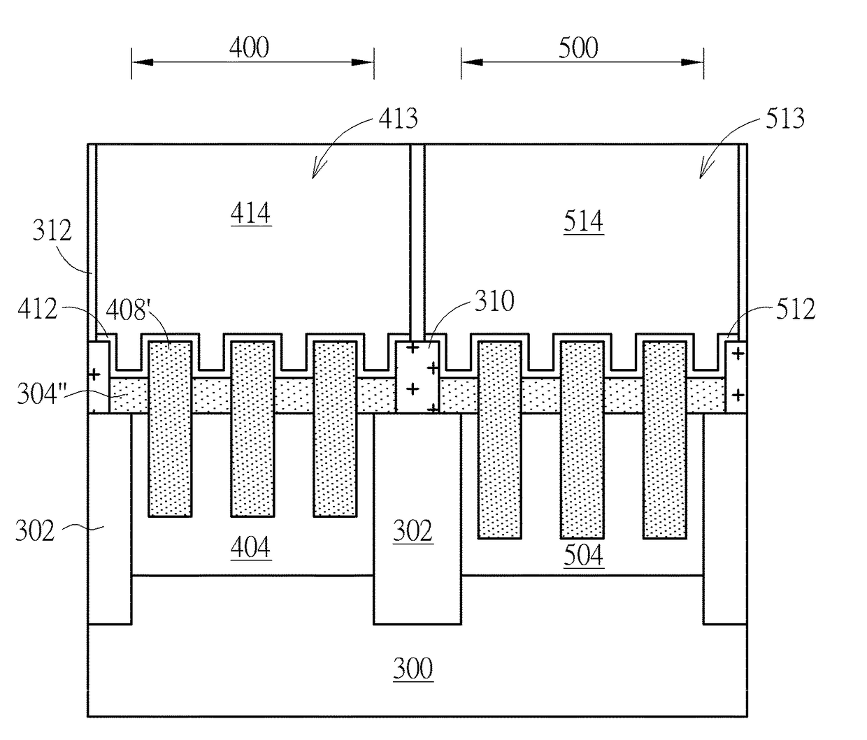
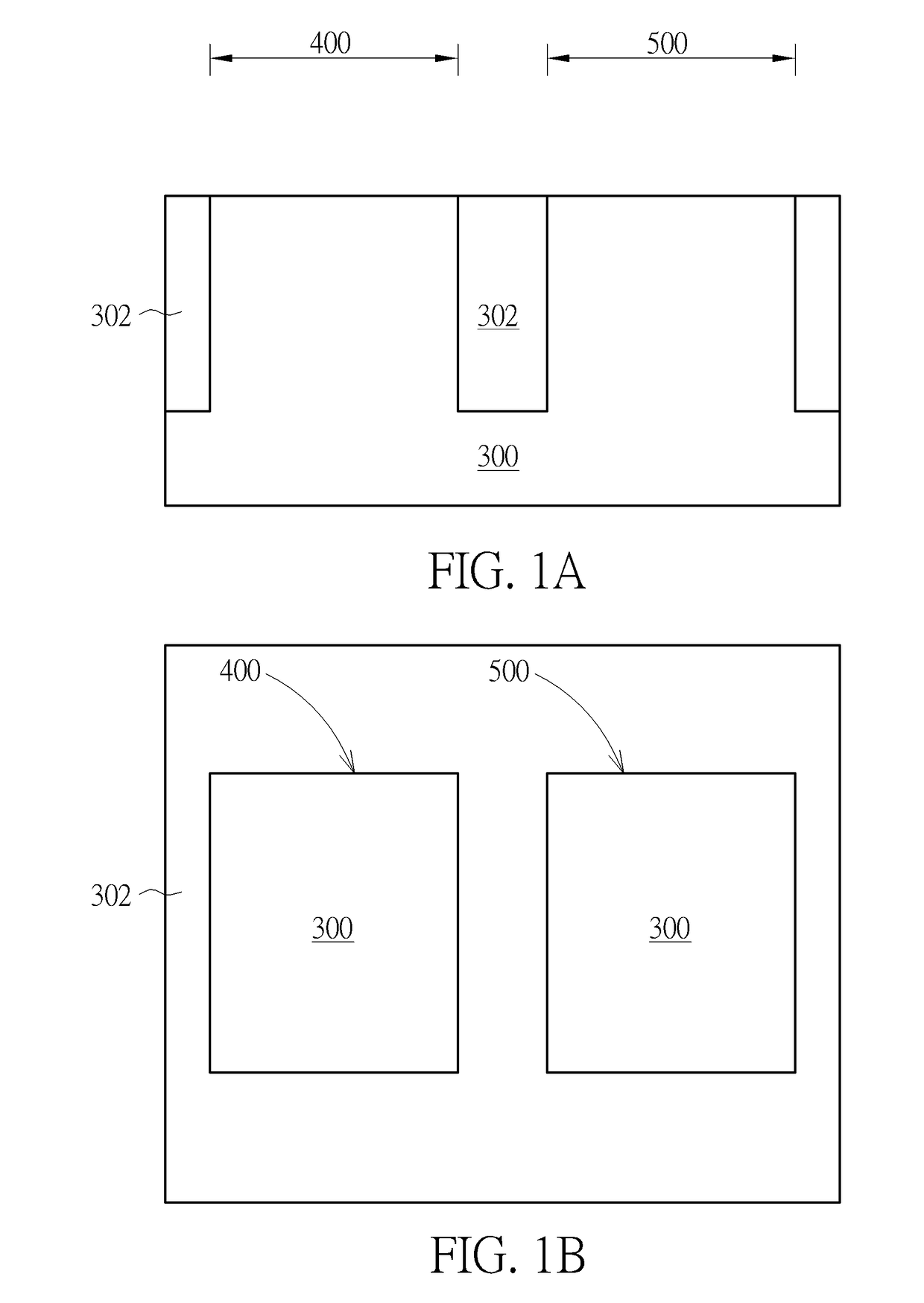
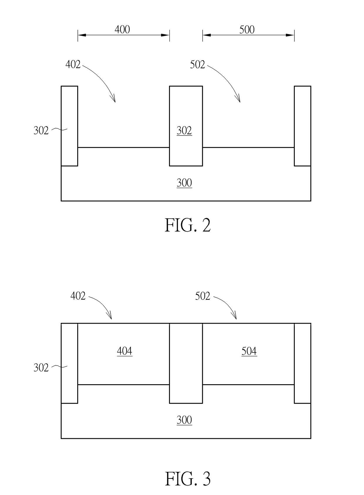
[0015]Please refer to FIG. 1A, FIG. 1B, FIG. 2, FIG. 3, FIG. 4A, FIG. 4B, FIG. 5A, FIG. 5B, FIG. 6A, FIG. 6B, FIG. 7A, FIG. 7B, FIG. 8A, FIG. 8B, FIG. 9A, FIG. 9B, FIG. 10A, FIG. 10B, FIG. 11A and FIG. 11B, which are schematic diagrams of the method of forming a semiconductor device according to one embodiment of the present invention, wherein FIG. 1A, FIG. 3, FIG. 4A, FIG. 5A, FIG. 6A, FIG. 7A, FIG. 8A, FIG. 9A, FIG. 10A and FIG. 11A are cross sectional view and FIG. 1B, FIG. 3B, FIG. 4B, FIG. 5B, FIG. 6B, FIG. 7B, FIG. 8B, FIG. 9B, FIG. 10B and FIG. 11B are top view.

[0016]Please first see FIG. 1A and FIG. 1B, wherein FIG. 1A is illustrated by taking along line AA′ of FIG. 1B. A semiconductor substrate 300 is provided to serve as a base for forming devi...


PUM


Abstract

The present invention provides a semiconductor device, including a substrate, a first semiconductor layer, a plurality of first sub recess, a plurality of insulation structures and a first top semiconductor layer. The substrate has a first region disposed within an STI. The first semiconductor layer is disposed in the first region. The first sub recesses are disposed in the first semiconductor layer. The insulation structures are disposed on the first semiconductor layer. The first top semiconductor layer forms a plurality of fin structures, which are embedded in the first sub recesses, arranged alternatively with the insulation structures and protruding over the insulation structures.

Description

CROSS REFERENCE TO RELATED APPLICATIONS[0001]This application is a Divisional of application Ser. No. 15 / 152,570 filed May 12, 2016, and included herein by reference.BACKGROUND OF THE INVENTION1. Field of the Invention[0002]The present invention relates to a semiconductor device and method of forming the same, and more particularly, relates to FinFET semiconductor device with fine lattice structure and method of forming the same.2. Description of the Prior Art[0003]In recent years, as various kinds of consumer electronic products are being constantly modified towards increased miniaturization, the size of semiconductor components are modified to be reduced accordingly, in order to meet high integration, high performance, low power consumption, and the demands of products.[0004]However, with the increasing miniaturization of electronic products, current planar FETs no longer meet the requirements of the products. Thus, non-planar FETs such as Fin-shaped FETs (Fin-FET) have been devel...

Claims


Application Information

Patent Timeline
Patent Type & Authority Applications(United States)
IPC IPC(8): H01L29/10H01L29/165H01L29/06H01L21/02H01L21/308H01L29/78H01L21/762H01L29/66
CPCH01L29/1054H01L29/165H01L29/0649H01L21/02634H01L21/3085H01L29/785H01L21/76278H01L29/66795H01L21/823431H01L29/6681H01L27/0886
Inventor TUNG, YU-CHENG
Owner UNITED MICROELECTRONICS CORP
Why Eureka
Try Eureka