

Method of forming semiconductor device
A semiconductor and device technology, which is applied in the field of semiconductor device formation, can solve the problems such as the electrical performance of semiconductor devices needs to be improved, achieve good electrical isolation performance, prevent the reduction of width and size, and reduce the effect of process difficulty
- Summary
- Abstract
- Description
- Claims
- Application Information
AI Technical Summary
Problems solved by technology
Method used
Image

Examples
Embodiment Construction
[0033] It is known from the background art that the electrical performance of semiconductor devices formed in the prior art needs to be improved.
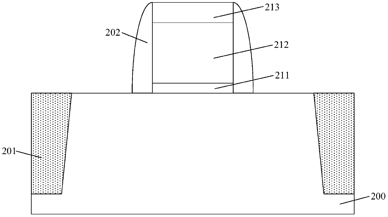
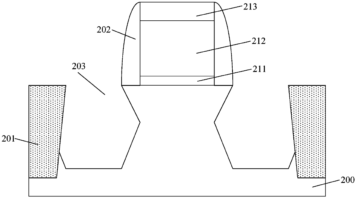
[0034] Research has found that in order to form embedded silicon germanium or embedded silicon carbon, it is usually necessary to etch the substrate on both sides of the gate structure in advance to form grooves; The impurities introduced by the etching process provide a good interface basis for the epitaxial stress layer; after cleaning, the epitaxial process is used to form a stress layer that fills the groove.
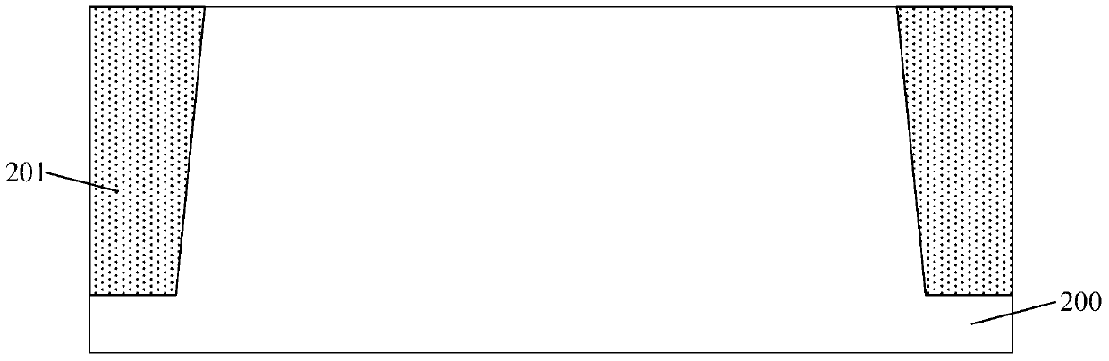
[0035] However, in general, there is an isolation structure in the substrate that plays an electrical isolation effect, and the filling material of the isolation structure is SiO 2 or SiON, and the groove will expose the sidewall surface of the isolation structure; and during the cleaning process, the cleaning process will 2Or SiON is etched, the cleaning process causes etching to the sidewall of the isolation structure...
PUM
 Abstract
Description
Claims
Application Information