Image processing apparatus, image processing method, and imaging system

a technology which is applied in the field of image processing apparatus and image processing method, and imaging system, can solve the problem of difficulty in only performing visible light imaging

Inactive Publication Date: 2018-10-25
SONY CORP
View PDF3 Cites 11 Cited by
  • Summary
  • Abstract
  • Description
  • Claims
  • Application Information

AI Technical Summary

Benefits of technology

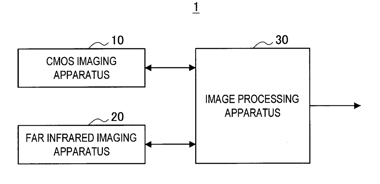
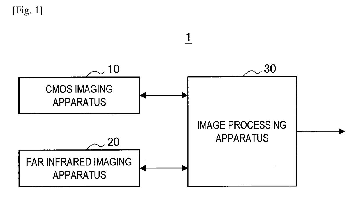
[0015]According to an embodiment of the present disclosure such as described above, it is possible to compensate the color or luminance of an image obtained based on an imaging element having sensitivity to near infrared light.

Problems solved by technology

It will be difficult to only perform imaging by visible light (light with a wavelength of 400 nm to 700 nm) in order to photograph brightly in a dark place.

Method used


Image

  • Image processing apparatus, image processing method, and imaging system
  • Image processing apparatus, image processing method, and imaging system
  • Image processing apparatus, image processing method, and imaging system

Examples


first modified example

5-1. First Modified Example

[0144]While an example has been described above in which an R pixel gain is decay compensated and the decay compensated R pixel gain is input to a color temperature estimation table, in order for the WB unit 16 to usually perform a light source color temperature estimation for an image signal in which the light receiving amount of an R pixel has increased, an embodiment of the present disclosure is not limited to such an example.

[0145]For example, the imaging system according to an embodiment of the present disclosure may prevent a light receiving amount increase of an R pixel, by inserting a notch filter (for example, a vapor deposited film or the like), which removes light of 700 nm to 800 nm, into the CMOS imaging apparatus 10. FIG. 19 is an explanatory diagram which shows spectral sensitivity characteristics of the CMOS sensor in the case where a notch filter has been inserted into the CMOS imaging apparatus 10. Since the solid line, the dotted line an...

second modified example

5-2. Second Modified Example

[0148]While an example has been described above in which a light source is not included in the imaging system 1, the imaging system according to an embodiment of the present disclosure may include a light source of near infrared light, for example, such as in the modified example shown below.

[0149]FIG. 20 is an explanatory diagram which shows a configuration of an imaging system 1′ including a near infrared light emission unit 40 which is a light source of near infrared light. Since the configuration other than the near infrared light emission unit 40 is the same as that of the imaging system 1 described with reference to FIG. 5, a description of this will be arbitrarily omitted.

[0150]The near infrared light emission unit 40 is an emission apparatus which emits near infrared light (for example light of 850 nm) capable of being received by the imaging element 12, for an imaging range of the CMOS imaging apparatus 10. By having the imaging system 1′ include...


PUM


Abstract

There is described an imaging method and an imaging device including first imaging circuitry that captures at least near infrared (NIR) light and outputs an NIR image, second imaging circuitry that captures far infrared (FIR) light and outputs an FIR image, wherein the FIR light has a longer wavelength than the NIR light, and processing circuitry configured to adjust color of the NIR image based on the FIR image.

Description

CROSS REFERENCE TO RELATED APPLICATIONS[0001]This application claims the benefit of Japanese Priority Patent Application JP 2014-246172 filed Dec. 4, 2014, the entire contents of which are incorporated herein by reference.TECHNICAL FIELD[0002]The present disclosure relates to an image processing apparatus, an image processing method, and an imaging system.BACKGROUND ART[0003]While a lighting condition is an important element in the case where performing photography by using an imaging apparatus such as a camera, the lighting condition will change significantly depending on the photographing environment. Further, since an appropriate image processing method will differ in accordance with the lighting condition, face region extraction technology has been disclosed, such as in PTL 1, for example, in which variations of the lighting condition are considered.[0004]On the other hand, in the fields of security cameras, vehicle cameras or the like, there is a demand for wanting to photograp...

Claims


Application Information

Patent Timeline
Patent Type & Authority Applications(United States)
IPC IPC(8): H04N5/33H04N9/44H04N9/64H04N9/04H04N9/09
CPCH04N5/33H04N9/44H04N9/64H04N9/0451H04N9/09H04N2209/048G06T3/4053G06T5/007G06T5/50G06T2207/10048G06T2207/30196G06T2207/30201H04N23/13H04N23/84
Inventor OKADA, SHUNJIKOSAKAI, RYOTAUKITA, SHINJIOBA, EIJIMASUZAWA, TSUYOSHIEBIHARA, MASAKAZUSHIMAUCHI, KAZUHIRO
Owner SONY CORP
Why Eureka
Try Eureka