Wafer level packaging method

a packaging method and wafer technology, applied in the field of semiconductor/solid-state device details, semiconductor devices, radiation controlled devices, etc., can solve the problem of often occurring unbonded problems, and achieve the effect of improving the yield of the wafer level packaging method

Active Publication Date: 2018-11-08
UNITED MICROELECTRONICS CORP
View PDF1 Cites 86 Cited by
  • Summary
  • Abstract
  • Description
  • Claims
  • Application Information

AI Technical Summary

Benefits of technology

[0024]As above, the first wafer and the second wafer are bonded together before the first wafer was trimmed. Therefore, an edge condition of the first wafer can be kept unchanged before the bonding step. As a result, an un-bonded problem at edge areas of the first wafer and the second wafer can be avoided, so that a yield of the wafer level packaging method can be improved. Furthermore, the trimming process performed to remove the lower chamfered edge of the

Problems solved by technology

However, an un-bonded problem often occurs during

Method used


Image

  • Wafer level packaging method
  • Wafer level packaging method
  • Wafer level packaging method

Examples


Embodiment Construction

[0030]Reference will now be made in detail to the present preferred embodiments of the invention, examples of which are illustrated in the accompanying drawings. Wherever possible, the same reference numbers are used in the drawings and the description to refer to the same or like parts.

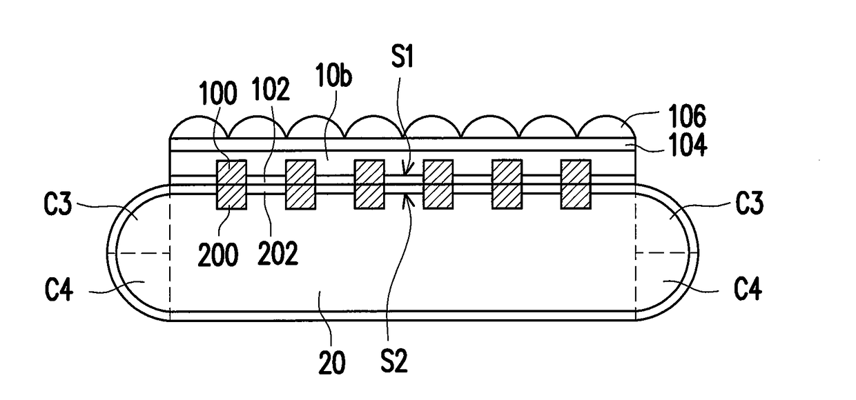
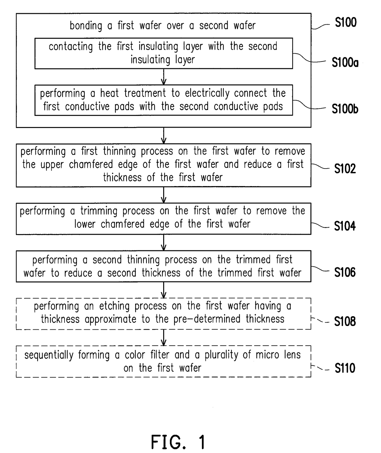
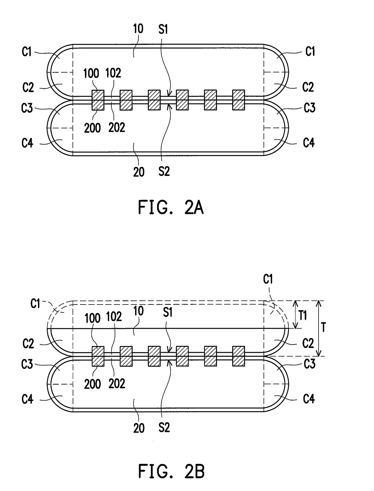
[0031]FIG. 1 is a flow chart illustrating a wafer level packaging method according to an embodiment of the invention. FIG. 2A through FIG. 2E are schematic cross-sectional views illustrating a wafer level packaging process according to an embodiment of the invention. FIG. 3 is a schematic cross-sectional view illustrating a sub-step of a process of bonding a first wader over a second wafer according to an embodiment of the invention. FIG. 4 is a schematic cross-sectional view illustrating a step of bonding a first wafer over a second wafer according to an alternative embodiment of the invention.

[0032]Referring to FIG. 1 and FIG. 2A, a wafer level packaging method of the present embodiment includes th...


PUM


Abstract

A wafer level packaging method includes the following steps. A first wafer is bonded over a second wafer. A first grinding process on the first wafer is performed, to remove an upper chamfered edge of the first wafer and reduce a thickness of the first wafer. A trimming process is performed on the first wafer, to remove a lower chamfered edge of the first wafer to form a trimmed first wafer. A second grinding process is performed on the trimmed first wafer, to reduce a thickness of the trimmed first wafer.

Description

BACKGROUND OF THE INVENTION1. Field of the Invention[0001]The present invention generally relates to a semiconductor packaging method, in particular, to a wafer level packaging method.2. Description of Related Art[0002]The wafer level packaging method has grown rapidly in the integrated circuit industry due to advantages in terms of the size of package structure as well as production time and cost. However, an un-bonded problem often occurs during a bonding step of the wafer level packaging method. To be more specific, a gap may exist between two bonded wafers at edge areas thereof. As a result, a yield of the wafer level packaging method may be lowered according to the un-bonded problem.SUMMARY OF THE INVENTION[0003]Accordingly, the present invention is directed to a wafer level packaging method that can avoid from the un-bonded problem.[0004]The invention provides a wafer level packaging method including the following steps. A first wafer is bonded over a second wafer. A first gri...

Claims


Application Information

Patent Timeline
IPC IPC(8): H01L27/146H01L21/306H01L23/00
CPCH01L27/1469H01L27/14687H01L2224/8084H01L21/30625H01L24/89H01L27/14685H01L2924/14H01L2924/10253H01L2924/13091H01L2924/10271H01L2924/10272H01L2924/10329H01L2924/12043H01L24/05H01L2224/08145H01L2224/80895H01L2224/80896H01L24/08H01L24/80H01L24/94H01L25/50H01L2224/05684H01L2224/05155H01L2224/05186H01L2224/05181H01L2224/05624H01L2224/05166H01L2224/05655H01L2224/05184H01L2224/05647H01L2224/05666H01L2224/2919H01L2924/00012H01L2924/013H01L2924/00014H01L2924/04941H01L2924/04953H01L2924/0496H01L2924/01074
Inventor ZHANG, SHENGDING, WEN-BOSHENG, ZHI-RUIHSU, CHIEN-ENPANG, CHIEN-KEE
Owner UNITED MICROELECTRONICS CORP
Why Eureka
Try Eureka