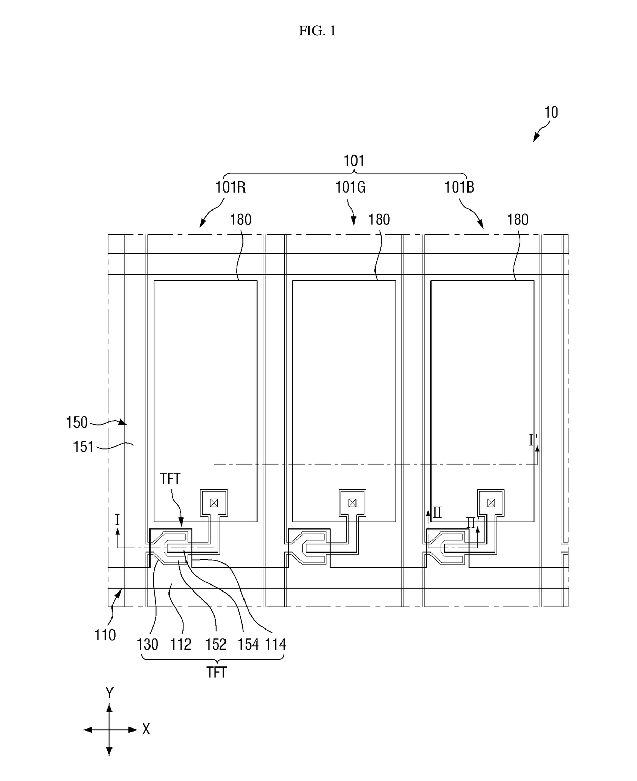
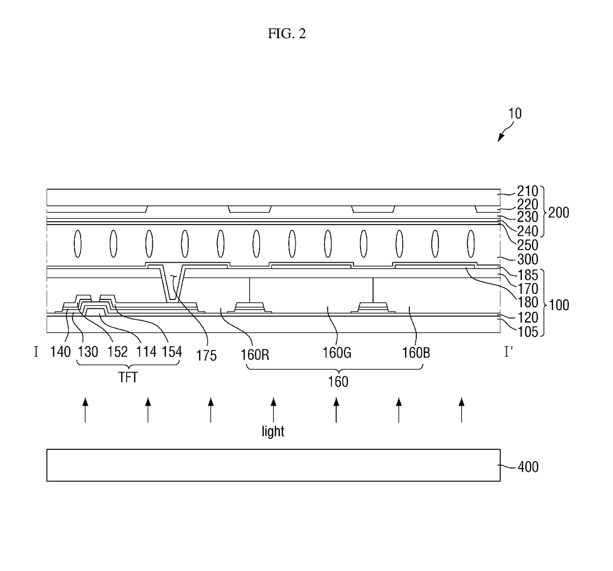
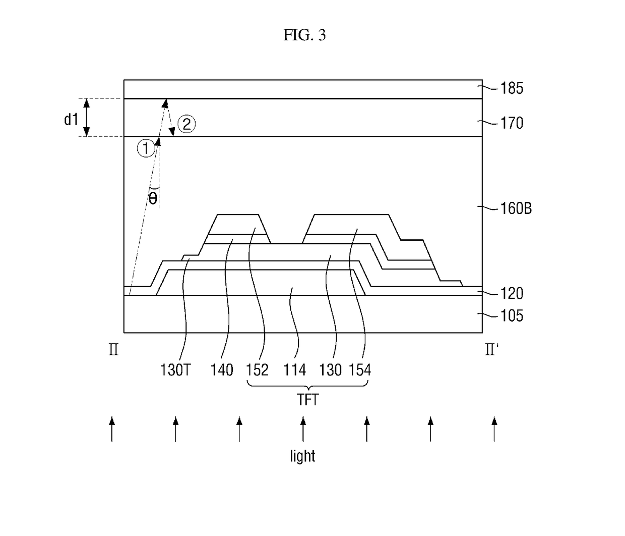
Display device

a display device and display technology, applied in semiconductor devices, instruments, optics, etc., can solve problems such as display defect in display devices, reduce leakage current caused by light incident on switching elements, improve switching operation of switching devices, and reduce display defects

Active Publication Date: 2018-11-29
SAMSUNG DISPLAY CO LTD
View PDF2 Cites 2 Cited by
  • Summary
  • Abstract
  • Description
  • Claims
  • Application Information

AI Technical Summary

Benefits of technology

This patent aims to improve the reliability of a display device by reducing leakage current caused by light incident on a switching element. This will result in less display defects and better operation of the switching device.

Problems solved by technology

As a result, a current may flow even when the switching element is turned off, such that a display defect may occur in the display device.

Method used


Image

  • Display device
  • Display device
  • Display device

Examples


Embodiment Construction

[0045]Advantages and features of the present inventive concept and methods of accomplishing the same may be understood more readily by reference to the following detailed description of preferred embodiments and the accompanying drawings. The present inventive concept may, however, be embodied in many different forms and should not be construed as being limited to the embodiments set forth herein. Rather, these embodiments are provided so that this disclosure will be thorough and complete and will fully convey the concept of the inventive concept to those skilled in the art, and the present inventive concept will only be defined by the appended claims.

[0046]It will also be understood that when a layer is referred to as being “on” another layer or substrate, it can be directly on the other layer or substrate, or intervening layers may also be present. The same reference numbers indicate the same components throughout the specification.

[0047]It will be understood that, although the te...


PUM

PropertyMeasurementUnit
refractive indexaaaaaaaaaa
refractive indicesaaaaaaaaaa

Abstract

The display device includes: a substrate; a thin-film transistor disposed on the substrate; a passivation layer covering the thin-film transistor; a capping layer disposed on the passivation layer; and a pixel electrode disposed on the capping layer and connected to the thin-film transistor, wherein a thickness of the capping layer is determined according to: d1=(λ / 2)×(1 / 2n), where d1 denotes the thickness of the capping layer, λ denotes a wavelength within visible wavelength range, and n denotes a ratio of refractive indices of the passivation layer to the capping layer.

Description

[0001]This application claims priority to Korean Patent Application No. 10-2017-0064166 filed on May 24, 2017 in the Korean Intellectual Property Office, the disclosure of which is incorporated herein by reference in its entirety.BACKGROUND1. Field of the Disclosure[0002]The present disclosure relates to a display device.2. Description of the Related Art[0003]Display devices display images and may be implemented as a liquid-crystal display (LCD) device, an organic light-emitting display (OLED) device, plasma display (PDP) device, an electrophoretic display (EPD) device, and electro-wetting display (EWD) device. Among these, LCD devices are widely used.[0004]An LCD device includes two display panels on which field generating electrodes such as a pixel electrode and a common electrode are formed, and a liquid-crystal layer disposed therebetween. In addition, the LCD device includes a backlight unit disposed below the display panels to provide light.[0005]Such an LCD device displays an...

Claims


Application Information

Patent Timeline
Patent Type & Authority Applications(United States)
IPC IPC(8): G02F1/1368
CPCG02F1/1368G02F2201/123G02F2001/136222G02F1/1337G02F1/136227G02F2201/50G02F2201/501G02F1/136222H01L27/1222H01L27/1248
Inventor OH, SE JOONKIM, SE JINLEE, YOUNG UOOKLEE, JUNG SULIM, SANG YEOULJUNG, SO MIJUNG, YOUNG MIN
Owner SAMSUNG DISPLAY CO LTD
Why Eureka
Try Eureka