Organic light emitting diode display device
- Summary
- Abstract
- Description
- Claims
- Application Information
AI Technical Summary
Benefits of technology
Problems solved by technology
Method used
Image


Examples
first embodiment
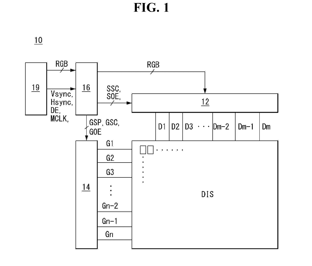
[0041]FIG. 3 is a cross-sectional view illustrating an organic light emitting diode display device according to a first embodiment of the present disclosure.
[0042]Referring to FIG. 3, an organic light emitting diode display device according to a first embodiment of the present disclosure includes a display panel having a first substrate SUB1 and a second substrate SUB2 facing each other and a conductive filler layer CFL interposed between the first substrate SUB1 and the second substrate SUB2. The first substrate SUB1 is a thin film transistor array substrate having a plurality of pixels in which a thin film transistor T and an organic light emitting diode OLE are arranged. The second substrate SUB2 is a substrate on which an Evss wiring EVL (or a low voltage level power wiring) is formed. The second substrate SUB2 can function as an encapsulation substrate. The first substrate SUB1 and the second substrate SUB2 may be bonded together through a sealant SL. The sealant SL may be disp...
second embodiment
[0067]FIG. 4 is a cross-sectional view illustrating an organic light emitting diode display device according to a second embodiment of the present disclosure. In describing the second embodiment, description of the substantially same parts as those of the first embodiment will be omitted.
[0068]Referring to FIG. 4, an organic light emitting diode display device according to a second embodiment of the present disclosure includes a display panel having a first substrate SUB1 and a second substrate SUB2 facing each other and a conductive filler layer CFL interposed between the first substrate SUB1 and the second substrate SUB2. The first substrate SUB1 is a thin film transistor array substrate in which a thin film transistor T and an organic light emitting diode OLE connected to the thin film transistor T are formed. The second substrate SUB2 is a substrate on which an Evss wiring EVL is formed.
[0069]Unlike the first embodiment, a color filter CF according to the second embodiment is fo...
third embodiment
[0070]FIG. 5 is a cross-sectional view illustrating an organic light emitting diode display device according to a third embodiment of the present disclosure. In describing the third embodiment, description of the substantially same parts as those of the first embodiment will be omitted.
[0071]Referring to FIG. 5, an organic light emitting diode display device according to a third embodiment of the present disclosure includes a display panel having a first substrate SUB1 and a second substrate SUB2 facing each other and a conductive filler layer CFL interposed between the first substrate SUB1 and the second substrate SUB2. The first substrate SUB1 is a thin film transistor array substrate in which a thin film transistor T and an organic light emitting diode OLE connected to the thin film transistor T are formed. The second substrate SUB2 is a substrate on which an Evss wiring EVL is formed.
[0072]The Evss wiring EVL and an auxiliary wiring AEVL are formed on the second substrate SUB2. ...
PUM
 Abstract
Description
Claims
Application Information