Dilute-Antimonide Group-II-Nitride Nanostructure Optoelectronic Devices

a technology of dilute-antimonide group and nano-nitride, which is applied in the direction of basic electric elements, semiconductor devices, electrical equipment, etc., can solve the problem of remained challenging to achieve efficient light emitter operating in the deep visible spectral rang

Active Publication Date: 2019-01-10
RGT UNIV OF MICHIGAN
View PDF0 Cites 2 Cited by
  • Summary
  • Abstract
  • Description
  • Claims
  • Application Information

AI Technical Summary

Problems solved by technology

However, it has remained challenging to achieve efficient light emitter operating in the deep visible spectral range.

Method used


Image

  • Dilute-Antimonide Group-II-Nitride Nanostructure Optoelectronic Devices
  • Dilute-Antimonide Group-II-Nitride Nanostructure Optoelectronic Devices
  • Dilute-Antimonide Group-II-Nitride Nanostructure Optoelectronic Devices

Examples


Embodiment Construction

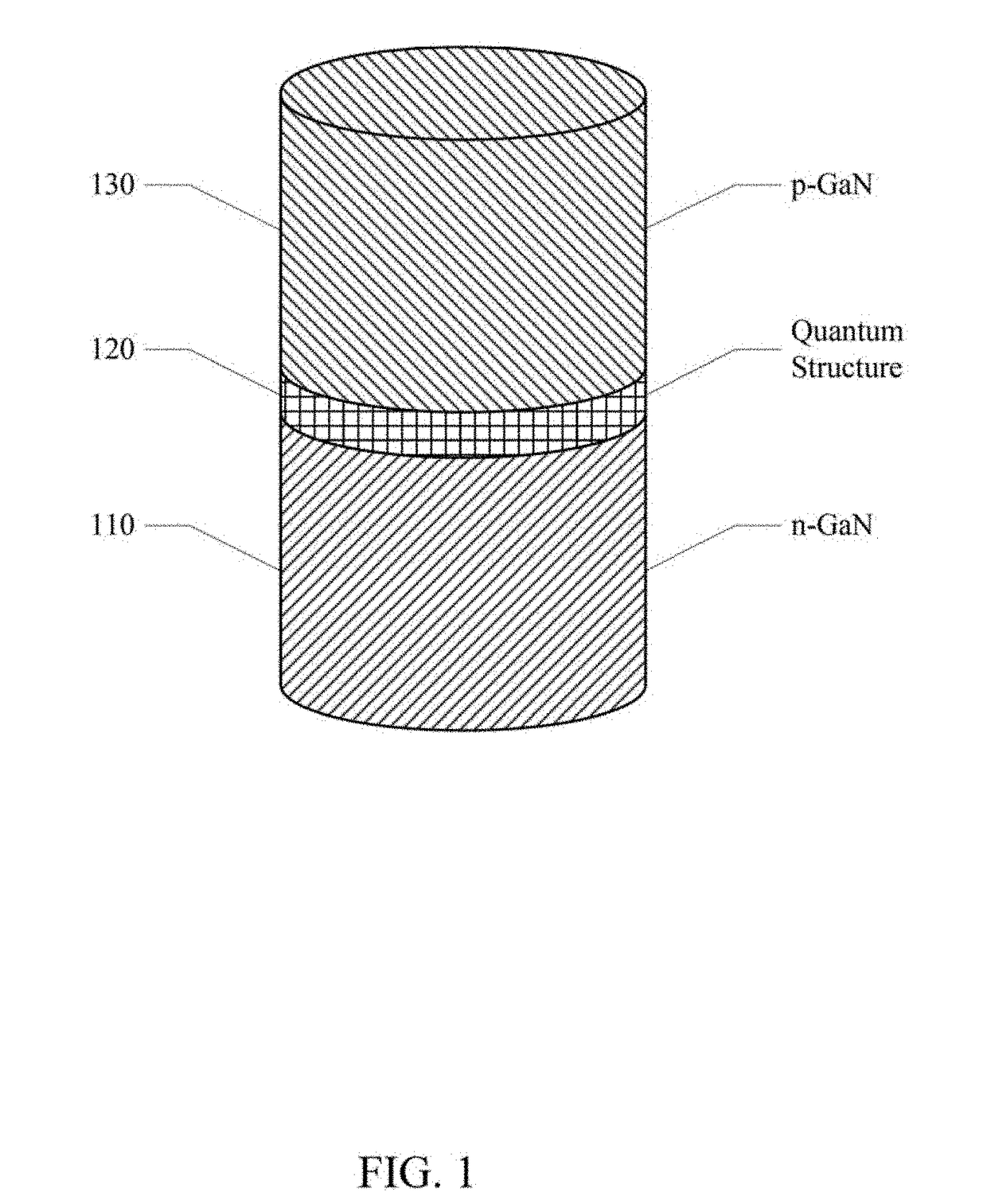
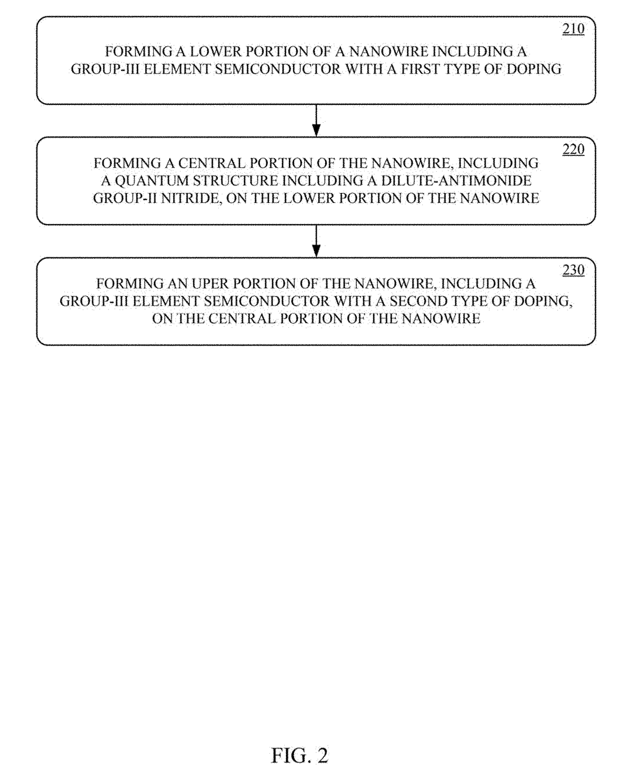
[0026]Reference will now be made in detail to the embodiment of the present technology, examples of which are illustrated in the accompanying drawings. While the present technology will be described in conjunction with these embodiments, it will be understood that they are not intended to limit the invention to these embodiments. On the contrary, the invention is intended to cover alternatives, modifications and equivalents, which may be included within the scope of the invention as defined by the appended claims. Furthermore, in the following detailed description of the present technology, numerous specific details are set forth in order to provide a thorough understanding of the present technology. However, it is understood that the present technology may be practiced without these specific details. In other instances, well-known methods, procedures, components, and circuits have not been described in detail as not to unnecessarily obscure aspects of the present technology.

[0027]S...


PUM


Abstract

A nanostructure optoelectronic device, in accordance with aspects of the present technology, can include a group-III element semiconductor with a first type of doping, one or more quantum structures including a dilute-Antimonide group-III-Nitride disposed on the first type of doped group-III element semiconductor, and a group-III element semiconductor with a second type of doping disposed on the dilute-Antimonide group-III-Nitride. The concentration of the Antimony (Sb) can be adjusted to vary the energy bandgap of the dilute-Antimonide group-III-Nitride between 3.4 and 2.0 electron Volts (eV)

Description

CROSS-REFERENCE TO RELATED APPLICATIONS[0001]This Application claims the benefit of U.S. Provisional Patent Application No. 62 / 529,915 filed Jul. 7, 2017, which is incorporated herein in its entirety.BACKGROUND OF THE INVENTION[0002]Computing systems have made significant contributions toward the advancement of modern society and are utilized in a number of applications to achieve advantageous results. Numerous devices, such as desktop personal computers (PCs), laptop PCs, tablet PCs, netbooks, smart phones, servers, and the like have facilitated increased productivity and reduced costs in communicating and analyzing data in most areas of entertainment, education, business, and science. One common aspect of computing device and other electronics are displays based on Light-Emitting Diodes (LEDs).[0003]Research in Gallium Nitride (GaN) based materials, including Indium Gallium Nitride (InGaN) Quantum Wells (QWs), has led to high brightness blue LEDs. However, it has remained challeng...

Claims


Application Information

Patent Timeline
Patent Type & Authority Applications(United States)
IPC IPC(8): H01L33/32H01L33/06H01L33/20H01L33/42H01L33/00H01L27/15H01L33/44
CPCH01L33/325H01L33/06H01L33/20H01L2933/0025H01L33/0075H01L27/156H01L33/44H01L33/42H01L33/08H01L33/18H01L33/24H01L33/32
Inventor CHOWDHURY, MOHAMMAD FAQRUL ALAMMI, ZETIAN
Owner RGT UNIV OF MICHIGAN
Why Eureka
Try Eureka