Sensor platform using a horizontally oriented nanotube element

a nanotube element and sensor technology, applied in the direction of microstructured devices, instruments, material impedances, etc., can solve the problems of inability to reliably manufacture nanoscale sensors using individual nanotubes, difficult control of individual nanotube placement between electrodes, and inability to detect target analytes

Active Publication Date: 2005-03-10
NANTERO
View PDF97 Cites 240 Cited by
  • Summary
  • Abstract
  • Description
  • Claims
  • Application Information

AI Technical Summary

Benefits of technology

[0032] Under certain embodiments of the invention, the support structure includes a conductive electrode positioned in the channel, and the sensor element is deflectable in response to the control circuitry to contact the electrode so that a gating effect of the nanotubes in the sensor element may be electrically detected.

Problems solved by technology

Because it is difficult to control the placement of individual nanotubes between electrodes, the reliable fabrication of nanoscale sensors using individual nanotubes is problematic.
Thus, devices using them may stop working if a single nanotube fails at a single point.

Method used


Image

  • Sensor platform using a horizontally oriented nanotube element
  • Sensor platform using a horizontally oriented nanotube element
  • Sensor platform using a horizontally oriented nanotube element

Examples


Embodiment Construction

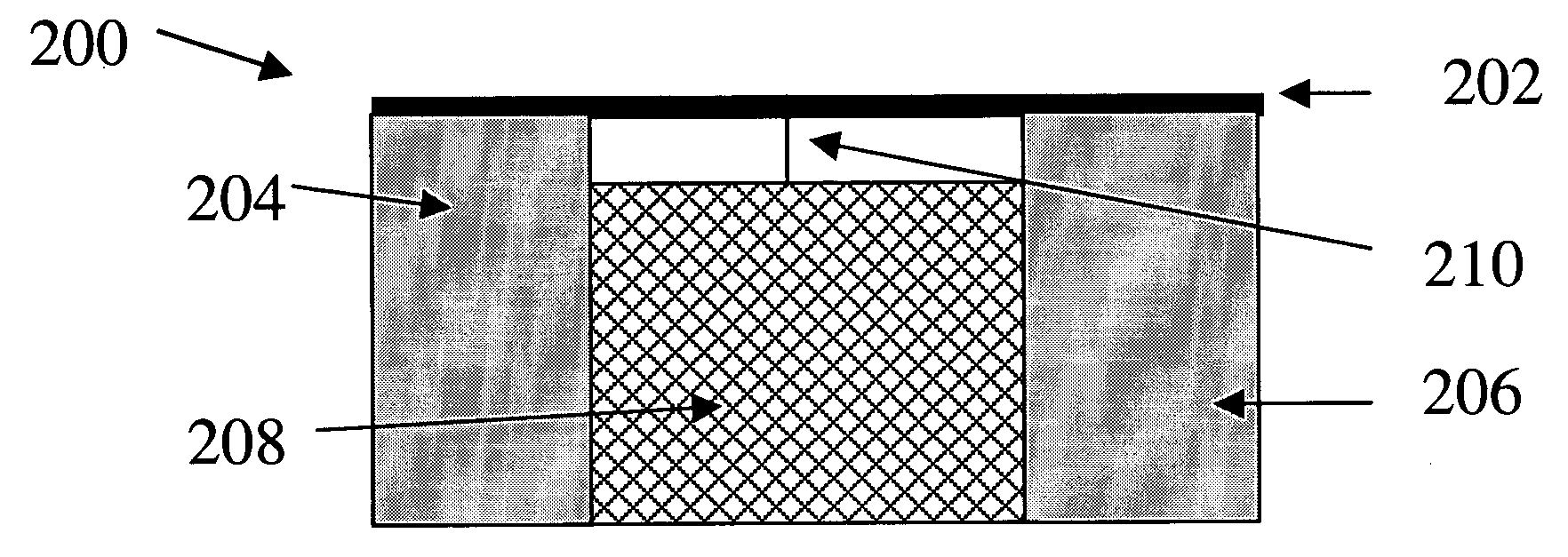
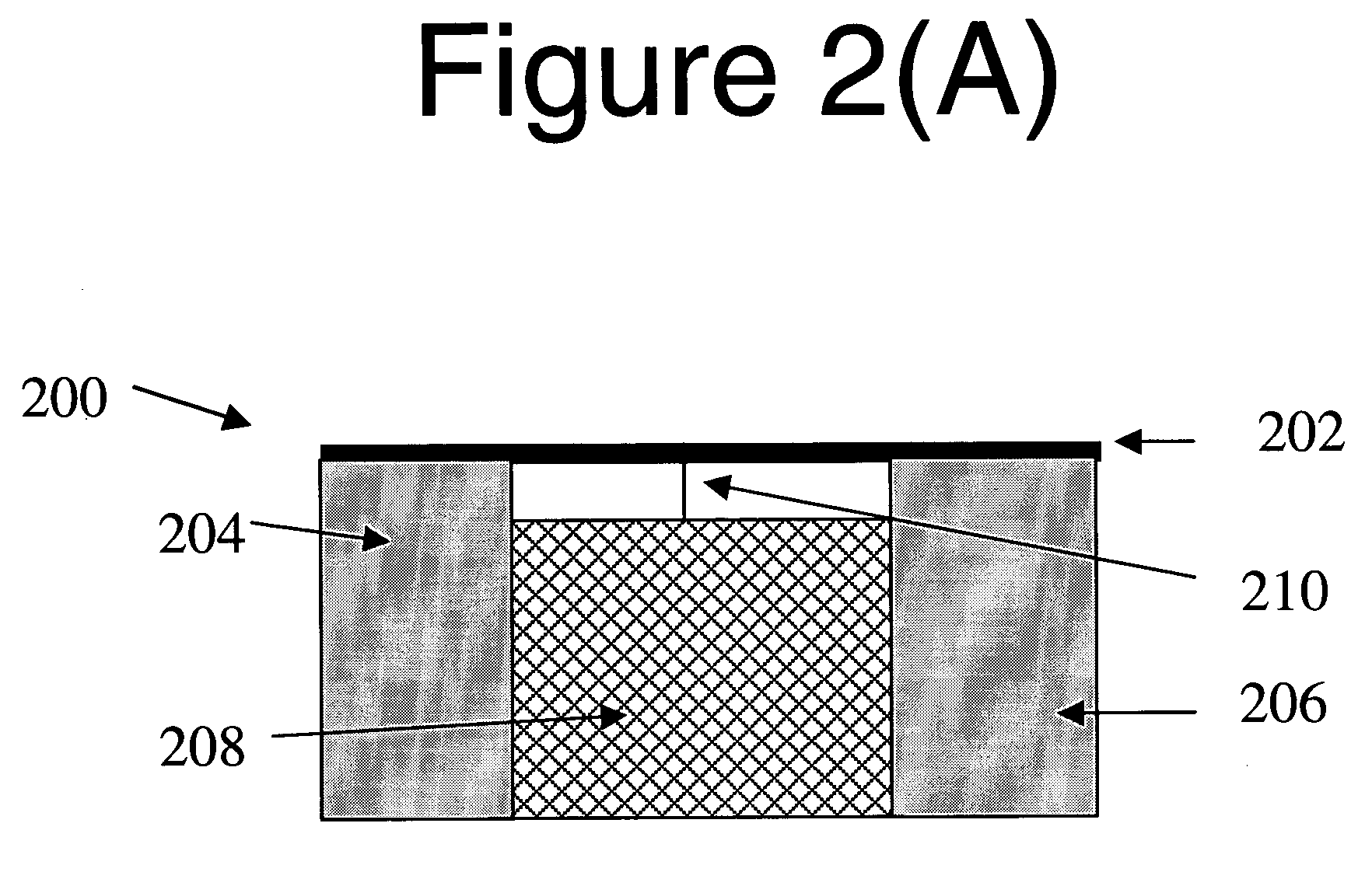
[0074] Preferred embodiments of the invention provide a new platform or vehicle to be used in sensors and sensor arrays for biological and / or chemical sensing. They can be built using conventional semiconductor fabrication techniques and can leverage existing manufacturing infrastructure and processes to create sensors employing carbon nanotubes. The manufacturing techniques are largely compatible with CMOS processes and can be conducted at lower temperatures than those for making prior-art nanotube sensing structures. They allow fabrication of a massive number of sensors on a given chip or wafer that can be integrated with various forms of control and computational circuitry.

[0075] As will be described in more detail below, preferred embodiments of the invention use elements made from a fabric of nanotubes (“nanofabrics”), rather than using individual nanotubes as was suggested in prior art. These elements may be derivatized or functionalized as is taught in the art for individual...


PUM

PropertyMeasurementUnit
diameteraaaaaaaaaa
gap distanceaaaaaaaaaa
widthaaaaaaaaaa

Abstract

Sensor platforms and methods of making them are described, and include platforms having horizontally oriented sensor elements comprising nanotubes or other nanostructures, such as nanowires. Under certain embodiments, a sensor element has an affinity for an analyte. Under certain embodiments, such a sensor element comprises one or more pristine nanotubes, and, under certain embodiments, it comprises derivatized or functionalized nanotubes. Under certain embodiments, a sensor is made by providing a support structure; providing a collection of nanotubes on the structure; defining a pattern within the nanotube collection; removing part of the collection so that a patterned collection remains to form a sensor element; and providing circuitry to electrically sense the sensor's electrical characterization. Under certain embodiments, the sensor element comprises pre-derivatized or pre-functionalized nanotubes. Under certain embodiments, sensor material is derivatized or functionalized after provision on the structure or after patterning. Under certain embodiments, a large-scale array includes multiple sensors.

Description

CROSS-REFERENCE TO RELATED APPLICATIONS [0001] This application claims priority to and the benefit of the filing dates of the following: [0002] Horizontally Oriented Sensor Constructed with Nanotube Technology (U.S. Provisional Pat. Appl., Ser. No. 60 / 470,410), filed May 14, 2003; [0003] Vertically Oriented Sensor Constructed with Nanotube Technology (U.S. Provisional Pat. Appl., Ser. No. 60 / 470,371), filed May 14, 2003; and [0004] Resistance and Capacitance Modulation Structures Constructed with Nanotube Technology (U.S. Provisional Pat. Appl., Ser. No. 60 / 501,143), filed Sep. 8, 2003. [0005] The following are assigned to the assignee of this application, and are hereby incorporated by reference in their entirety: [0006] Nanotube Films and Articles (U.S. patent application Ser. No. 10 / 128,118), filed Apr. 23, 2002; [0007] Electromechanical Memory Array Using Nanotube Ribbons and Method for Making Same (U.S. patent application Ser. No. 09 / 915,093), filed on Jul. 25, 2001; [0008] Ele...

Claims


Application Information

Patent Timeline
Patent Type & Authority Applications(United States)
IPC IPC(8): B81B3/00G01N27/00G01N27/02G01N27/12G01N27/22G01N27/414G01N33/487G01R15/00
CPCB82Y15/00G11C13/025Y10S977/92Y10S977/902Y10S977/904Y10T29/49082Y10S977/921Y10S977/922G01N27/4146Y10T29/43Y10S977/924
Inventor SEGAL, BRENT M.RUECKES, THOMASVOGELI, BERNHARDBROCK, DARRENJAIPRAKASH, VENKATACHALAM C.BERTIN, CLAUDE L.
Owner NANTERO
Why Eureka
Try Eureka