Nanocomposites

a technology of nanocomposites and composite materials, applied in the field of nanocomposites, can solve the problems of difficult formation of thin uniform films, difficult to find single component materials possessing these properties, and difficult to form into thin uniform films used in many microelectronics applications, etc., to achieve efficient waveguided, increase the percentage of re-emitted light, and improve the index of refraction

Active Publication Date: 2006-06-27
ONED MATERIAL INC
View PDF47 Cites 247 Cited by
  • Summary
  • Abstract
  • Description
  • Claims
  • Application Information

AI Technical Summary

Benefits of technology

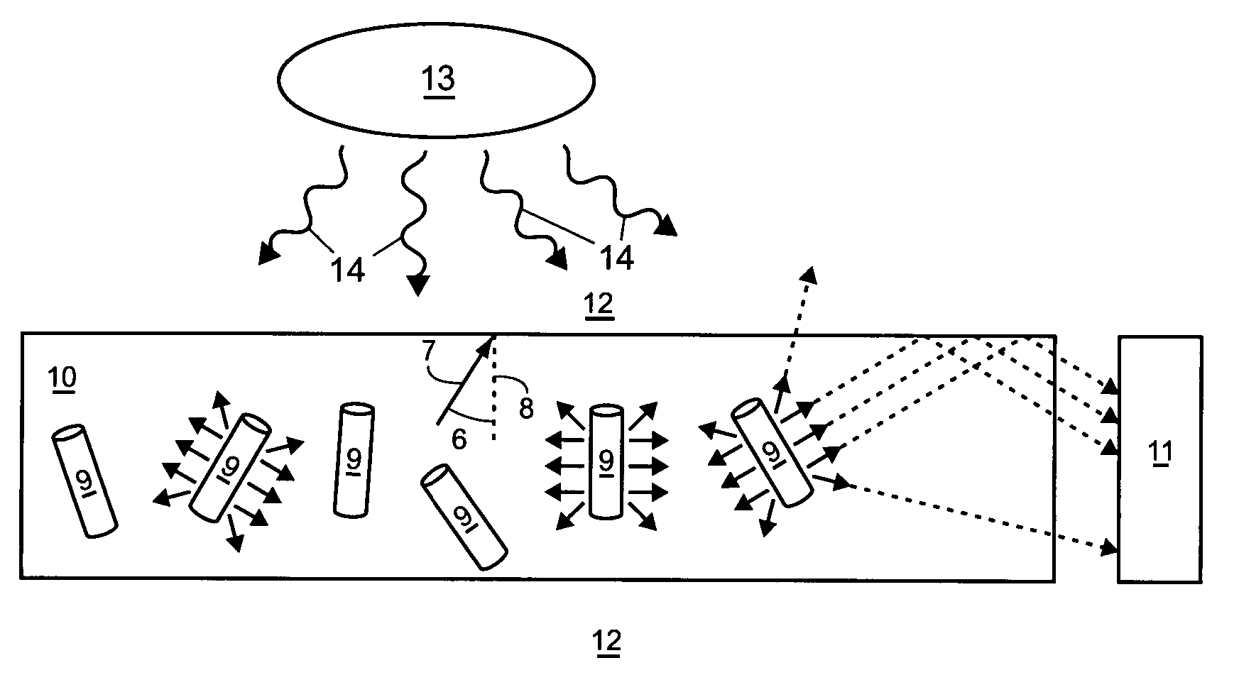
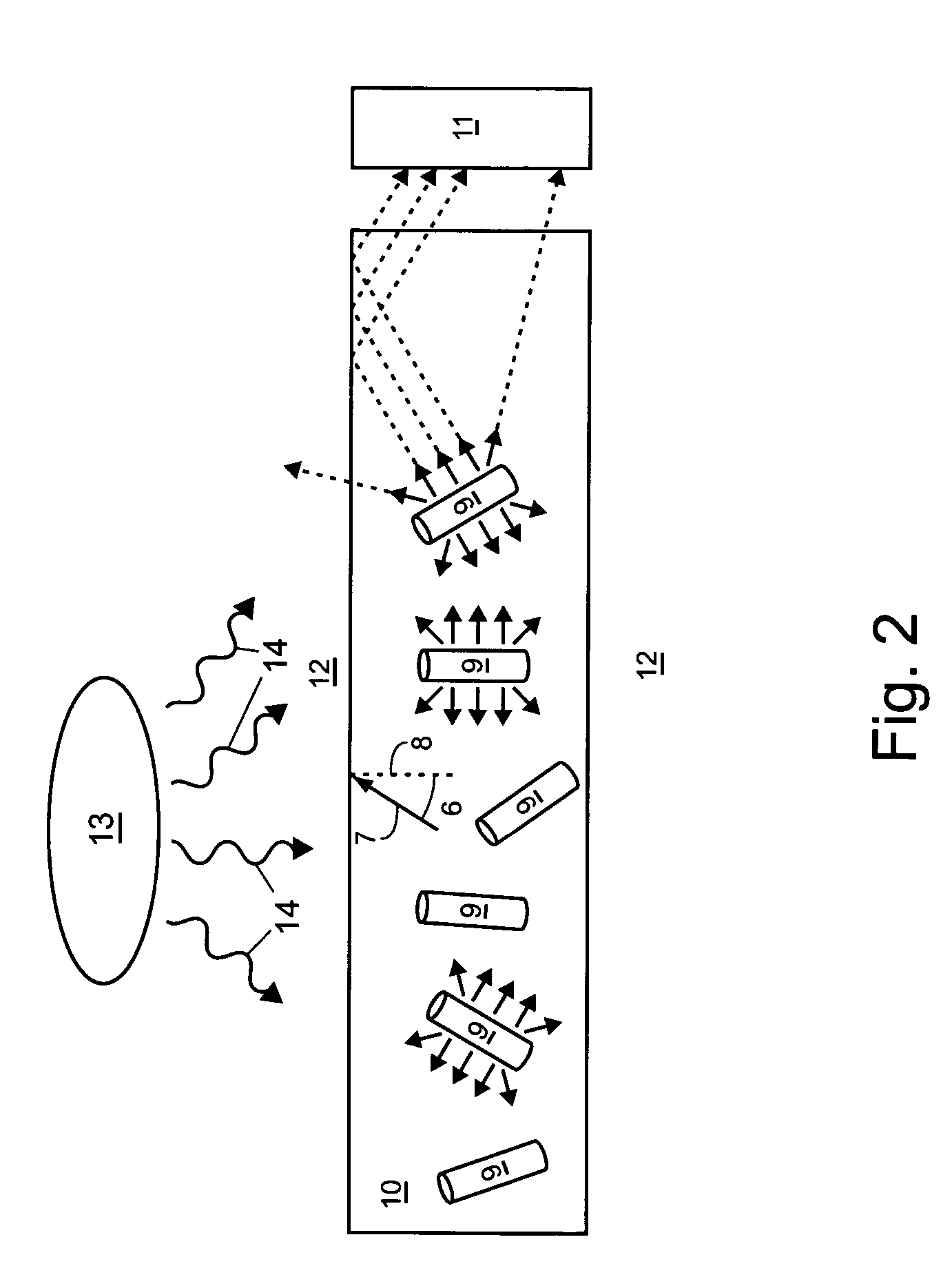
[0009]One aspect of the invention provides waveguides and light concentrators comprising nanostructures, which in some but not all embodiments are provided as part of a nanocomposite. The nanostructures absorb light impinging on the waveguide or light concentrator and re-emit light. The nanostructures can be located and / or oriented within the waveguide or light concentrator in a manner that increases the percentage of re-emitted light that can be waveguided. For example, the nanostructures can be located and / or oriented within a light concentrator in such a manner that a greater percentage of the reemitted light is waveguided (and can thus be collected at the edge of the concentrator) than would be waveguided if emission by the collection of nanostructures were isotropic (equal in every direction).
[0010]One class of embodiments provides a waveguide comprising a cladding (e.g., a material that has a lower refractive index than the core, e.g., a lower refractive index solid, liquid, or gas, e.g., air) and a core, where the core comprises one or more nanowires or branched nanowires (e.g., nanotetrapods) and a matrix. The first and second surfaces of the core are substantially parallel so light emitted by the nanowires or branched nanowires can be efficiently waveguided by total internal reflection, and the core has a higher index of refraction than the cladding, for a similar reason. The nanowires or branched nanowires can comprise essentially any convenient material (e.g., a fluorescent material, a semiconducting material) and can comprise essentially a single material or can be heterostructures. The size of the nanostructures (e.g., the diameter and / or aspect ratio of nanowires) can be varied. In embodiments in which the core comprises a plurality of nanowires, the nanowires can be either randomly or substantially nonrandomly oriented (e.g., with a majority of the nanowires being more nearly perpendicular than parallel to a surface of the core, or with the nanowires forming a liquid crystal phase). Nonrandom orientation of the nanowires can increase the efficiency of the waveguide by increasing the percentage of light that is reemitted at angles greater than the critical angle for the particular core-cladding combination. The waveguides can be connected to a collector for collecting waveguided light, and can be used in stacks to form a multilayer light concentrator, in which the different layers comprise waveguides that can be optimized to collect light of different wavelengths.
[0011]Another class of embodiments provides a waveguide comprising a cladding (e.g., a material that has a lower refractive index than the core, e.g., a lower refractive index solid, liquid, or gas, e.g., air), a first core, and a first layer that comprises one or more nanostructures. The first layer is distributed on but is not necessarily in contact with the first core, whose first and second surfaces are substantially parallel. Some embodiments further comprise a second core. The first layer can be in direct contact with the first and / or second core(s), or can be separated from either or both, e.g., by a layer of a material whose refractive index is between that of the first layer and the core. The first layer preferably has a thickness less than about one wavelength of the light emitted by the nanostructures. The nanostructures can be nanowires, nanocrystals, or branched nanowires (e.g., nanotetrapods). The nanostructures can comprise essentially any convenient material (e.g., a fluorescent material, a semiconducting material) and can comprise essentially a single material or can be heterostructures. The size of the nanostructures (e.g., the diameter and / or aspect ratio of nanowires) can be varied. The nanostructures can be provided in various manners, e.g., as substantially pure nanostructures or as part of a nanocomposite. In embodiments in which the waveguide comprises a plurality of nanowires, the nanowires can be either randomly or substantially nonrandomly oriented (e.g., with a majority of the nanowires being more nearly perpendicular than parallel to a surface of the first core, or with the nanowires forming a liquid crystal phase). Nonrandom orientation of the nanowires can increase the efficiency of the waveguide by increasing the percentage of light that is reemitted at angles greater than the critical angle. The waveguides can be connected to a collector for collecting waveguided light, and can be used in stacks to form a multilayer light concentrator, in which the different layers comprise waveguides that can be optimized to collect light of different wavelengths.

Problems solved by technology

Finding single component materials possessing these properties is difficult.
For example, high dielectric constant ceramic materials such as ferroelectric SrTiO3, BaTiO3, or CaTiO3 are brittle and are processed at high temperatures that are incompatible with current microcircuit manufacturing processes, while polymer materials are very easy to process but have low dielectric constants.
For example, they are difficult to form into the thin uniform films used for many microelectronics applications.
Unfortunately, at the moment neither of these strategies is effective.
The complexity of increased-efficiency solar cells causes their cost to be substantially greater than the increase in performance.
Similarly, larger solar panels are proportionately more expensive due to difficulties in fabricating uniform devices over large areas.

Method used


Image

  • Nanocomposites
  • Nanocomposites
  • Nanocomposites

Examples


Embodiment Construction

[0047]Composite materials comprising nanostructures (nanocomposites) are provided, along with articles comprising nanocomposites and methods and compositions for making such composites.

[0048]One class of embodiments provides waveguides and light concentrators comprising nanostructures. This class of embodiments is based on the ability of certain nanostructures (e.g., nanostructures comprising a fluorescent material) to absorb and re-emit light that can then be waveguided by total internal reflection within at least one core. In many but not all embodiments, the nanostructures are provided in the form of a nanocomposite. In some embodiments, the nanostructures are substantially nonrandomly oriented to increase the efficiency of the waveguide or light concentrator.

[0049]Methods for orienting nanostructures within a composite material are discussed, including using the matrix or components thereof to orient the nanostructures. Accordingly, one aspect of the invention provides nanocompo...


PUM

PropertyMeasurementUnit
aspect ratioaaaaaaaaaa
aspect ratiosaaaaaaaaaa

Abstract

This invention provides composite materials comprising nanostructures (e.g., nanowires, branched nanowires, nanotetrapods, nanocrystals, and nanoparticles). Methods and compositions for making such nanocomposites are also provided, as are articles comprising such composites. Waveguides and light concentrators comprising nanostructures (not necessarily as part of a nanocomposite) are additional features of the invention.

Description

CROSS REFERENCE TO RELATED APPLICATIONS[0001]This application claims priority to and benefit of U.S. Provisional Patent Application No. 60 / 408,722, filed Sep. 5, 2002, “Nanocomposites” Mihai Buretea et al., which is incorporated herein by reference in its entirety for all purposes.FIELD OF THE INVENTION[0002]The present invention is in the field of nanocomposites. More particularly, the invention includes composite materials comprising nanostructures (e.g., nanowires, nanorods, branched nanowires, nanotetrapods, nanocrystals, quantum dots, and nanoparticles), methods and compositions for making such composites, and articles comprising such composites. Waveguides and light concentrators comprising nanostructures that are not necessarily part of a nanocomposite are also features of the invention.BACKGROUND OF THE INVENTION[0003]A composite material (a composite) is formed by combining two or more materials that have different properties. The composite typically has properties differen...

Claims


Application Information

Patent Timeline
Patent Type & Authority Patents(United States)
IPC IPC(8): G02B5/10F24S23/00G02B1/04G02B6/122H01S3/063H01S5/10
CPCB82Y20/00H01L31/0547C03C14/006C08L83/04F24J2/067G02B1/045H01L31/055H01S3/0632B82Y30/00C08L83/00C03C2214/16G02F2202/36H01S3/169H01S5/10Y02E10/40Y02E10/52Y10T428/29F24S23/12
Inventor BURETEA, MIHAIEMPEDOCLES, STEPHENNIU, CHUNMINGSCHER, ERIK C.
Owner ONED MATERIAL INC
Why Eureka
Try Eureka