

Post-deposition encapsulation of nanostructures: compositions, devices and systems incorporating same
a nanostructure and encapsulation technology, applied in the field of nanotechnology, can solve the problems of large and/or disordered and/or low density packing nanoparticles, high cost (high temperature, high vacuum), and the thickness of the nanostructure generated by these and other standard core-shell synthetic techniques is not thick enough to confine a charge in the core. , to achieve the effect of reducing or preventing other types of transmission, reducing the rate of charge diffusion, and reducing the rate of charg
- Summary
- Abstract
- Description
- Claims
- Application Information
AI Technical Summary
Benefits of technology
Problems solved by technology
Method used
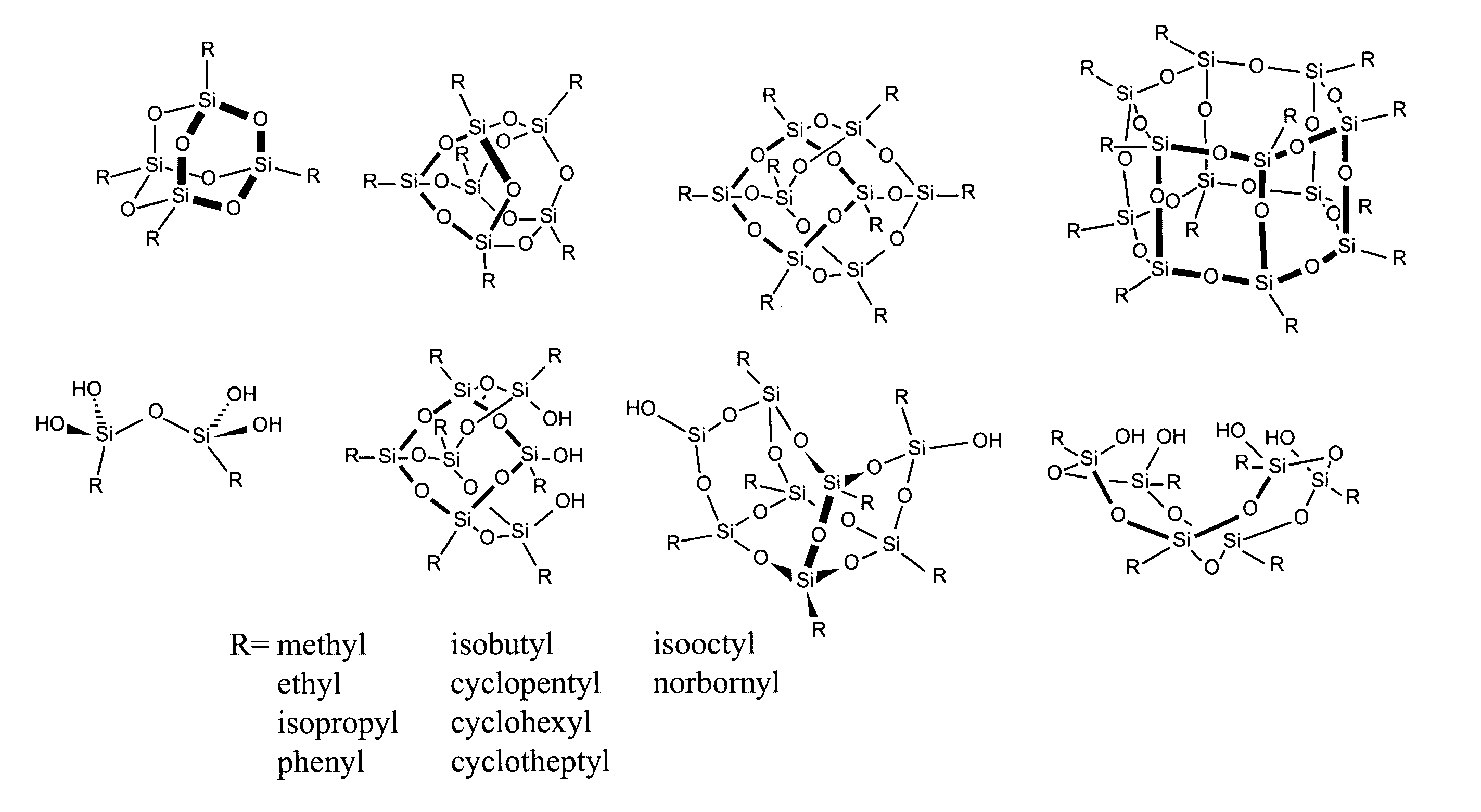
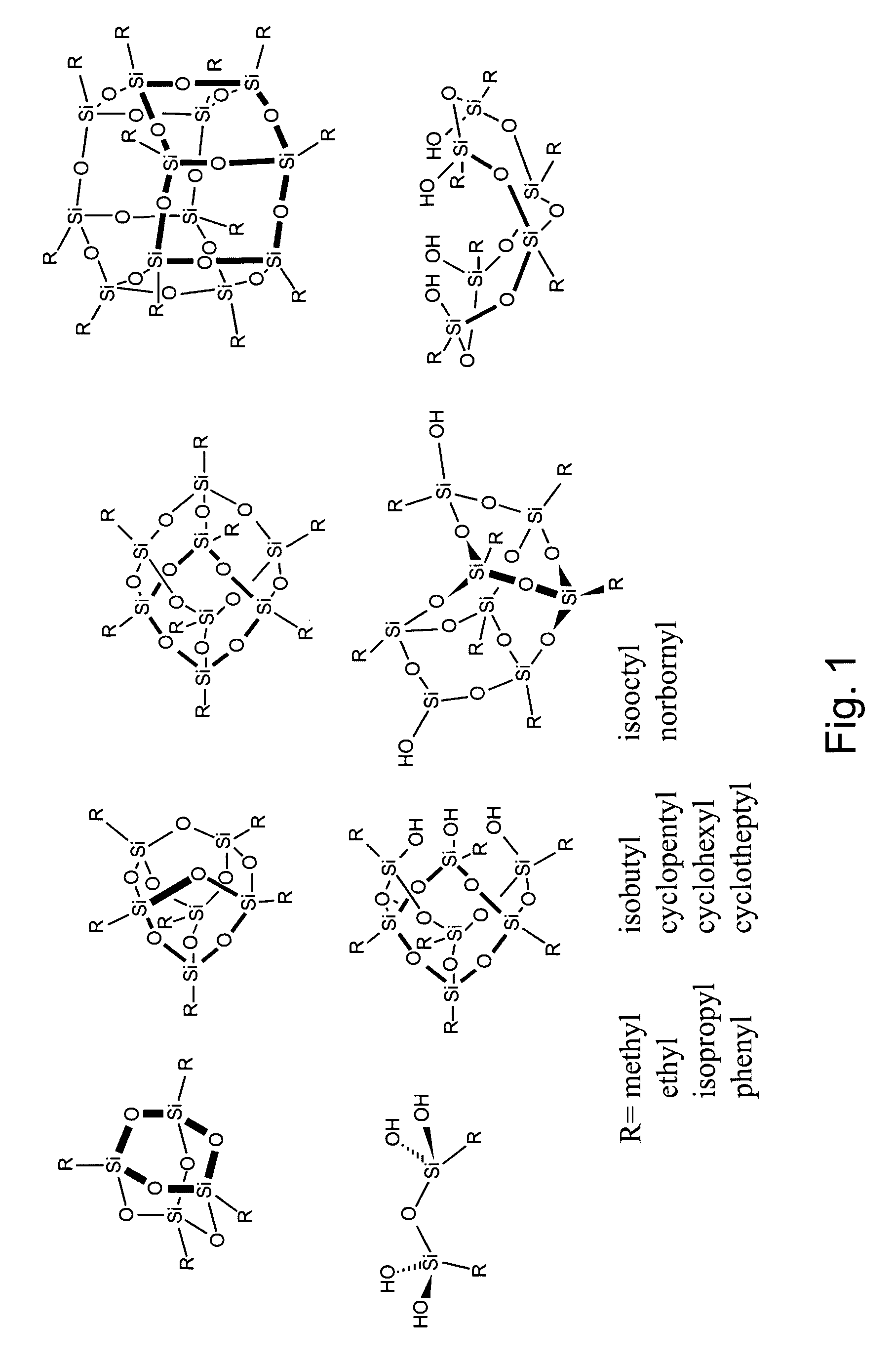
Image

Examples
example 1
Preparation of Closely Packed Nanostructure Monolayers
[0158] A method for preparing a substrate having closely packed nanostructures is depicted schematically in FIGS. 3 and 4. A nanodot (depicted as a sphere) is synthesized with surfactants that coat the surface. The surfactants are ligand-exchanged for the silsesquioxane or other silicate ligand (L).
[0159] A selected substrate (e.g., a silicon dioxide wafer) is coated with a silane ligand bearing a nanostructure binding head group (B). The silane ligands interact and associate into a self assembled monolayer of surface assembly ligand (SAL) on the substrate surface, providing a nanostructure-binding interface (as indicated by the perpendicular arrows). An exemplary surface assembly ligand includes a cyclic dimethyl amino moiety and a SiMe2 group coupled together via a linker (cyclic dimethyl amino-organic spacer-SiMe2).
[0160] The ligand exchanged nanodots are then put on the SAL substrate by spin coating or dip coating with the...
example 2
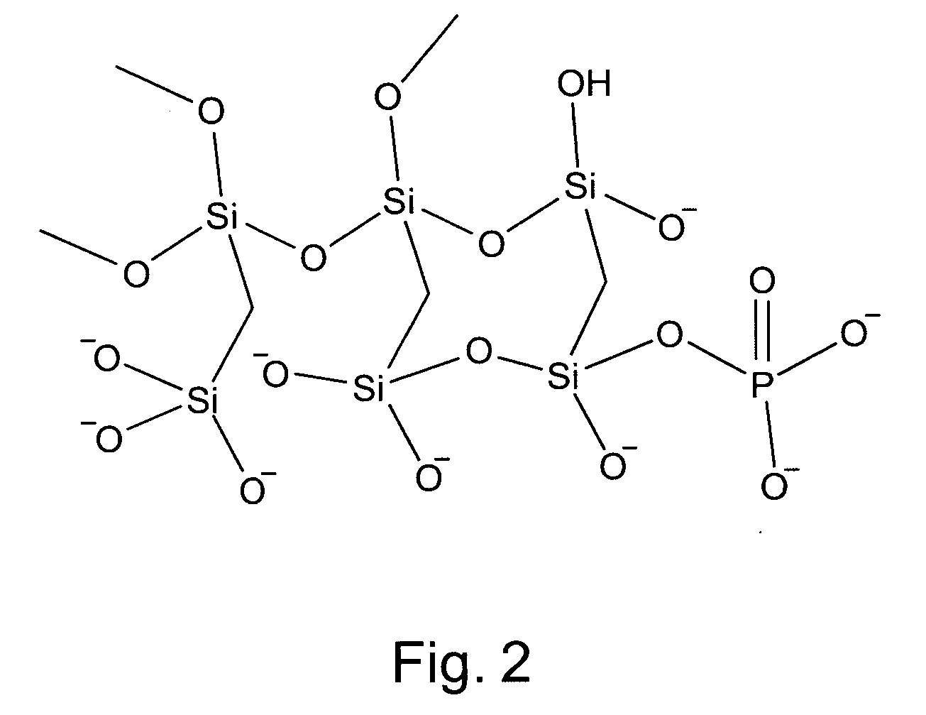
Synthesis of Heptacyclopentyl POSS Disilanol Diethoxyphosphate
[0161] Synthesis of the exemplary polyhedral oligomeric silsesquioxane (POSS) ligand heptacyclopentyl POSS disilanol diethoxyphosphate 2 was performed as provided herein (FIG. 6). All procedures were carried out under an inert atmosphere using Schlenk technique. The solvents were dried over 4 Å molecular sieves and degassed with three freeze-vacuum-thaw cycles. The heptacyclopentyl POSS trisilanol 1 was dried by static vacuum in a dessicator with phosphorous pentoxide for 12 hours, and diethyl chlorophosphonate (Cl—P(O)(OEt)2 was vacuum transferred before use. Mass spectrometry was performed at Scripps Research Institute in La Jolla, and 31P {1H} NMR spectroscopy was performed with a Bruker FT NMR using 31P at 162 MHz.
[0162] The reaction was set up in a 50 mL Schlenk flask. Heptacyclopentyl POSS trisilanol 1 (1.00 g, 1.14 mmol) was dissolved in a combination of toluene (10 mL) and triethylamine (15 mL) and produced a cl...
example 3
Generation of a Monolayer of Coated Nanostructures On a SAM
[0170] The controlled self-assembly of monolayers of nanocrystals with silsesquioxane or silicate ligands tailored for charge storage applications can be achieved by various wet-process methods, such as the deposition onto self-assembled monolayers (SAMs). This approach can be used to prepare monolayers having close packed nanostructure arrays, and preferably ordered close-packed nanostructure arrays.
[0171] A self assembled monolayer consisting of a silane ligand with a binding head for the silsesquioxane or silicate ligand is applied to a substrate surface. The nanocrystals are deposited on the SAM from solution by spin-, dip-, or spray-coating, or conventional printing technologies. The excess dots are washed off the substrate resulting in a monolayer of nanocrystals insulated with silicon dioxide containing ligands.
PUM
| Property | Measurement | Unit |
|---|---|---|
| diameter | aaaaa | aaaaa |
| diameter | aaaaa | aaaaa |
| diameter | aaaaa | aaaaa |
Abstract
Description
Claims
Application Information