

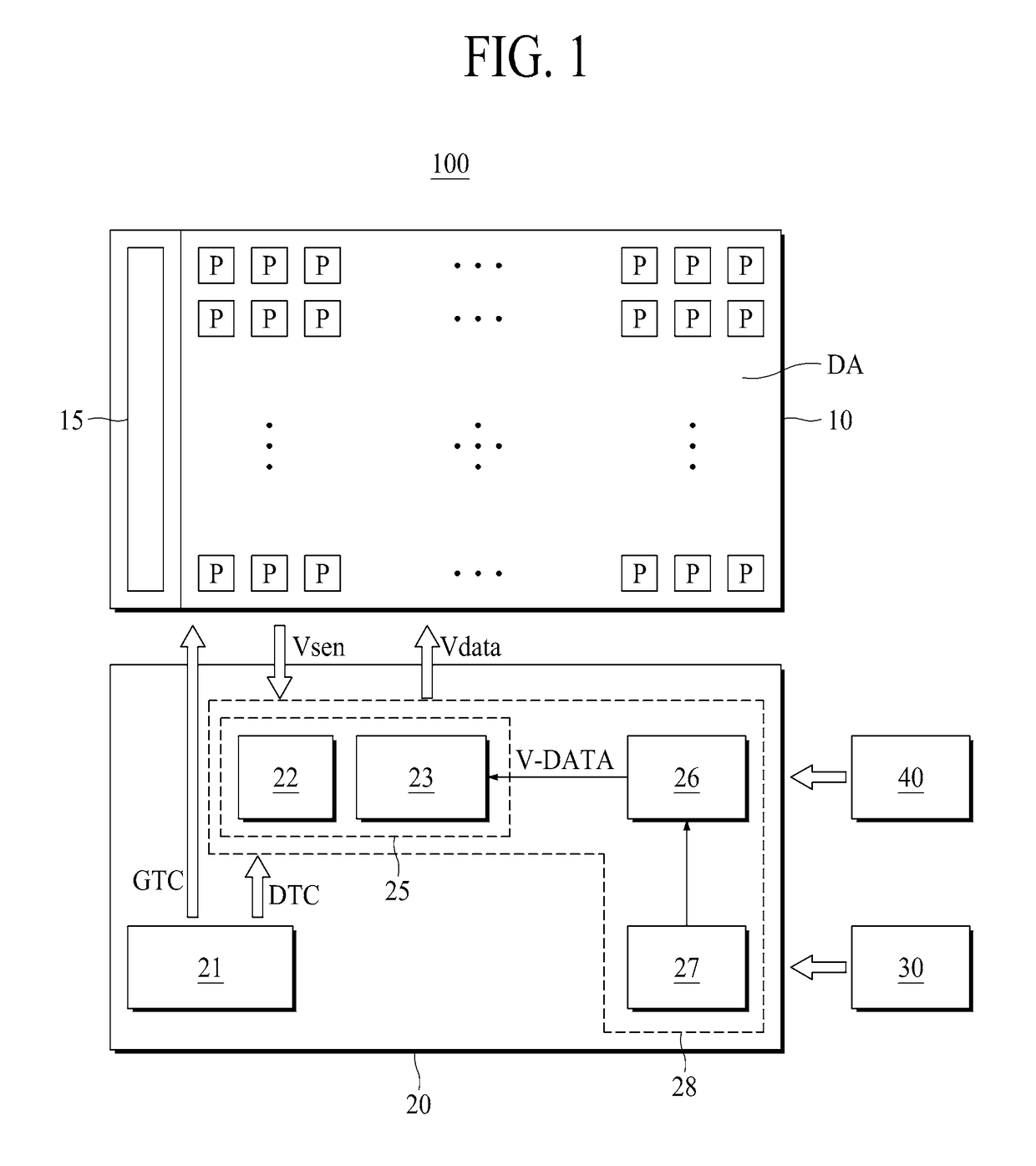
Gate Driving Circuit and Display Device Including the Same
a driving circuit and display device technology, applied in the direction of electrical devices, semiconductor devices, instruments, etc., can solve the problems of difficult implementation of narrow-bezel display devices, long data updating period, flicker, etc., to enhance reliability, enhance reliability, enhance the effect of gate driving circuit reliability
- Summary
- Abstract
- Description
- Claims
- Application Information
AI Technical Summary
Benefits of technology
Problems solved by technology
Method used
Image

Examples
first embodiment
[0091]FIG. 5 is a circuit diagram illustrating a first scan driving circuit according to the present disclosure. In detail, the first scan driving circuit configures each of a plurality of first scan stages, and the circuit diagram of FIG. 5 is a detailed circuit diagram of FIG. 4. FIG. 6 is a waveform diagram of the first scan driving circuit illustrated in FIG. 5 and is a waveform diagram when a QB node operates during one horizontal period 1H.
[0092]Referring to FIG. 5, all of a plurality of transistors configuring the first scan stages may be p-type transistors. The first scan stages may each include a first transistor T1, a second transistor T2, a third transistor T3, and a fourth transistor T4. A gate electrode of the first transistor T1 may be connected to a Q node Q, and a gate electrode of the second transistor T2 may be connected to a QB node QB. The Q node Q may charge the gate electrode of the first transistor T1, and the QB node QB may discharge the gate electrode of the...
second embodiment
[0118]FIG. 7 is a circuit diagram illustrating a first scan driving circuit according to the present disclosure. In detail, the first scan driving circuit configures each of a plurality of first scan stages, and the circuit diagram of FIG. 7 is a detailed circuit diagram of FIG. 4. FIG. 8 is a waveform diagram of the first scan driving circuit illustrated in FIG. 7 and is a waveform diagram when a QB node operates during one horizontal period 1H. FIG. 7 illustrates a modification embodiment of the first scan driving circuit of FIG. 5, and thus, description repetitive of FIG. 5 is omitted or will be briefly described. For example, an nth first scan stage will be described below with reference to FIG. 7.
[0119]Referring to FIG. 7, as described above with reference to FIG. 5, a second gate low voltage VGL2 which is higher than a first gate low voltage VGL1 may be applied to a first electrode of a fourth transistor T4, for turning on the fourth transistor T4. The second gate low voltage ...
third embodiment
[0123]FIG. 9 is a circuit diagram illustrating a first scan driving circuit according to the present disclosure. In detail, the first scan driving circuit configures each of a plurality of first scan stages, and the circuit diagram of FIG. 9 is a detailed circuit diagram of FIG. 4. FIG. 10 is a waveform diagram of the first scan driving circuit illustrated in FIG. 9 and is a waveform diagram when a QB node operates during two horizontal periods 2H.
[0124]Referring to FIG. 9, the first scan stages may each include a first transistor T1, a second transistor T2, a third transistor T3, and a fourth transistor T4. A gate electrode of the first transistor T1 may be connected to a Q node Q, and a gate electrode of the second transistor T2 may be connected to a QB node QB. The Q node Q may charge the gate electrode of the first transistor T1, and the QB node QB may discharge the gate electrode of the second transistor T2. In this case, since the transistors configuring the first scan stages ...
PUM
 Abstract
Description
Claims
Application Information