Time borrowing between layers of a three dimensional chip stack

a three-dimensional chip and chip stack technology, applied in the field of machine learning, can solve the problems of not being able to implement machine-trained networks with as much progress in circuits, and achieve the effect of facilitating time borrowing

Active Publication Date: 2019-02-07
XCELSIS CORP
View PDF0 Cites 25 Cited by
  • Summary
  • Abstract
  • Description
  • Claims
  • Application Information

AI Technical Summary

Benefits of technology

[0003]Unlike a flip-flop that releases in one clock cycle a signal that it stores in a prior clock cycle, a transparent latch does not introduce such a setup time delay in the design. In fact, by allowing the signal to pass through the first circuit partition to the second circuit partition during its open mode, the latch allows the signal to borrow time from a first portion of a clock cycle of the second circuit partition for a second portion of the clock cycle of the second circuit partition. This borrowing of time is referred to below as time borrowing. Also, this time borrowing allows the signal to be available at the destination node in the second circuit partition early so that the second circuit can act on it in the clock cycle that this signal is needed. Compared to flip-flops, latches also reduce the clock load because, while flip-flops require at least two different clock transitions to store and then release a value, transparent latches only require one signal transition to latch a value that they previously passed through.

Problems solved by technology

However, there has not been as much advances in circuits for implementing machine-trained networks.

Method used


Image

  • Time borrowing between layers of a three dimensional chip stack
  • Time borrowing between layers of a three dimensional chip stack
  • Time borrowing between layers of a three dimensional chip stack

Examples


Embodiment Construction

[0035]In the following detailed description of the invention, numerous details, examples, and embodiments of the invention are set forth and described. However, it will be clear and apparent to one skilled in the art that the invention is not limited to the embodiments set forth and that the invention may be practiced without some of the specific details and examples discussed.

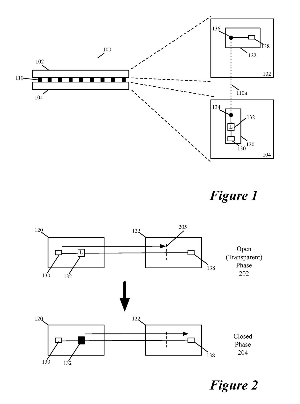
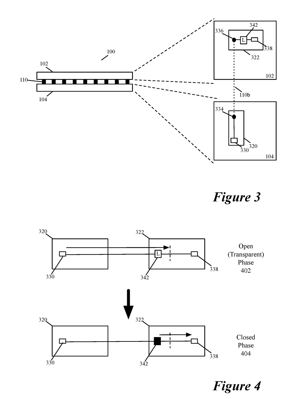
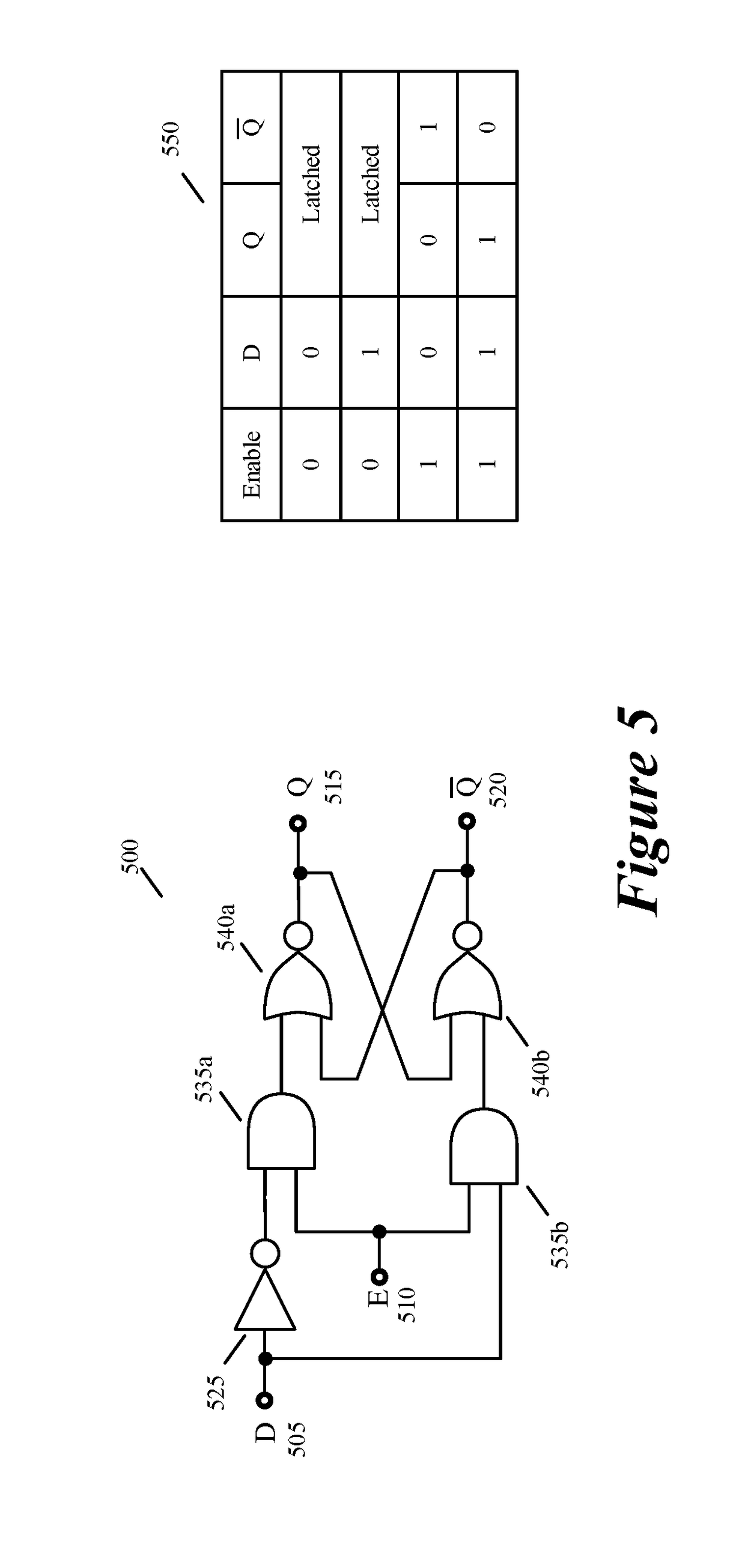
[0036]Some embodiments of the invention provide a three-dimensional (3D) circuit structure that uses latches to transfer signals between two bonded circuit layers. In some embodiments, this structure includes a first circuit partition on a first bonded layer and a second circuit partition on a second bonded layer. It also includes at least one latch to transfer signals between the first circuit partition on the first bonded layer and the second circuit partition on the second bonded layer. In some embodiments, the latch operates in (1) an open first mode (also called a transparent mode) that allows a signal to...


PUM


Abstract

Some embodiments of the invention provide a three-dimensional (3D) circuit structure that uses latches to transfer signals between two bonded circuit layers. In some embodiments, this structure includes a first circuit partition on a first bonded layer and a second circuit partition on a second bonded layer. It also includes at least one latch to transfer signals between the first circuit partition on the first bonded layer and the second circuit partition on the second bonded layer. In some embodiments, the latch operates in (1) an open first mode that allows a signal to pass from the first circuit partition to the second circuit partition and (2) a closed second mode that maintains the signal passed through during the prior open first mode. By allowing the signal to pass through the first circuit partition to the second circuit partition during its open mode, the latch allows the signal to borrow time from a first portion of a clock cycle of the second circuit partition for a second portion of the clock cycle of the second circuit partition.

Description

BACKGROUND[0001]In recent years, there have been great advances in the field of machine learning. Much of these advances have been in machine trained networks (e.g., deep neural networks) and algorithms for training such networks. However, there has not been as much advances in circuits for implementing machine-trained networks. This has been primarily due to an over reliance on implementing machine trained networks in datacenters as opposed to in devices in the real world. Therefore, there is a need in the art for innovative circuits for implementing machine trained networks as well as other types of designs.BRIEF SUMMARY[0002]Some embodiments of the invention provide a three-dimensional (3D) circuit structure that uses latches to transfer signals between two bonded circuit layers. In some embodiments, this structure includes a first circuit partition on a first bonded layer and a second circuit partition on a second bonded layer. It also includes at least one latch to transfer sig...

Claims


Application Information

Patent Timeline
Patent Type & Authority Applications(United States)
IPC IPC(8): G06N3/04G06N3/08G06N3/063H01L25/065H01L23/31
CPCG06N3/04G06N3/082G06N3/063H01L25/0657H01L23/3128H01L2225/06513H01L2225/06517H01L24/16H01L2224/16145H01L2224/16225H01L2225/06586H01L2225/06541H03K19/21H01L2225/06565H01L24/17H01L2224/16227H01L2224/17181H01L2924/16235G06N3/084G06F11/1423G06F11/2028G06F11/2041G06F11/2051G06N3/048G06N3/08H01L25/0756H01L25/043H01L2225/06503H01L25/117H01L25/074G06N3/065G06F11/2007G06F2201/85H01L2225/06524H01L2225/06582
Inventor TEIG, STEVEN L.DUONG, KENNETHDELACRUZ, JAVIER
Owner XCELSIS CORP
Why Eureka
Try Eureka