Semiconductor package device and method of manufacturing the same
- Summary
- Abstract
- Description
- Claims
- Application Information
AI Technical Summary
Benefits of technology
Problems solved by technology
Method used
Image

Examples
Embodiment Construction
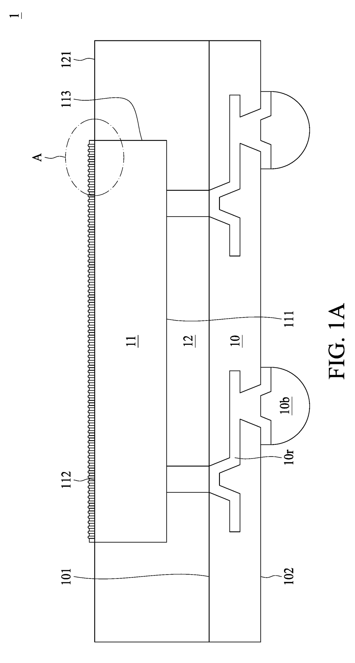
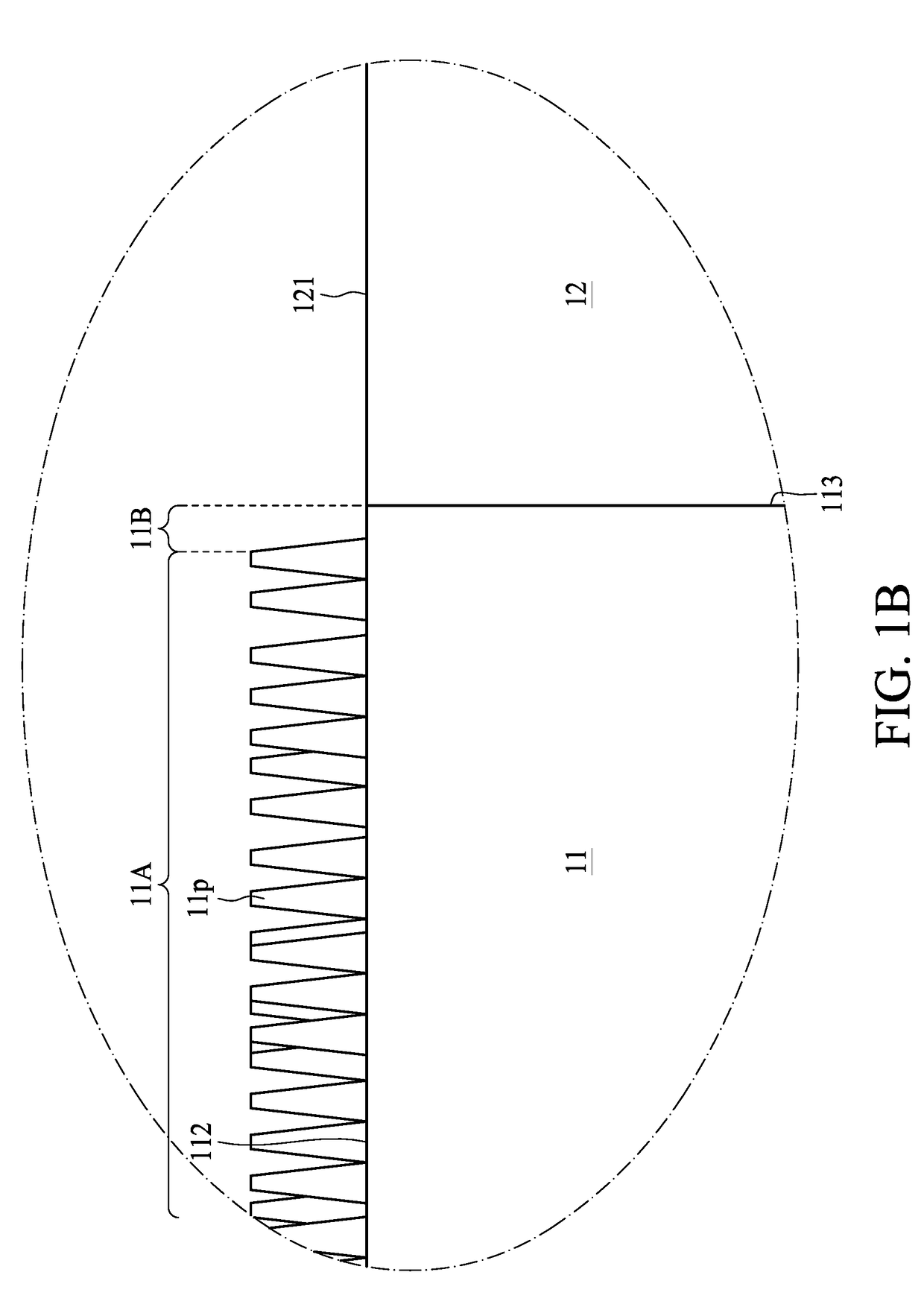
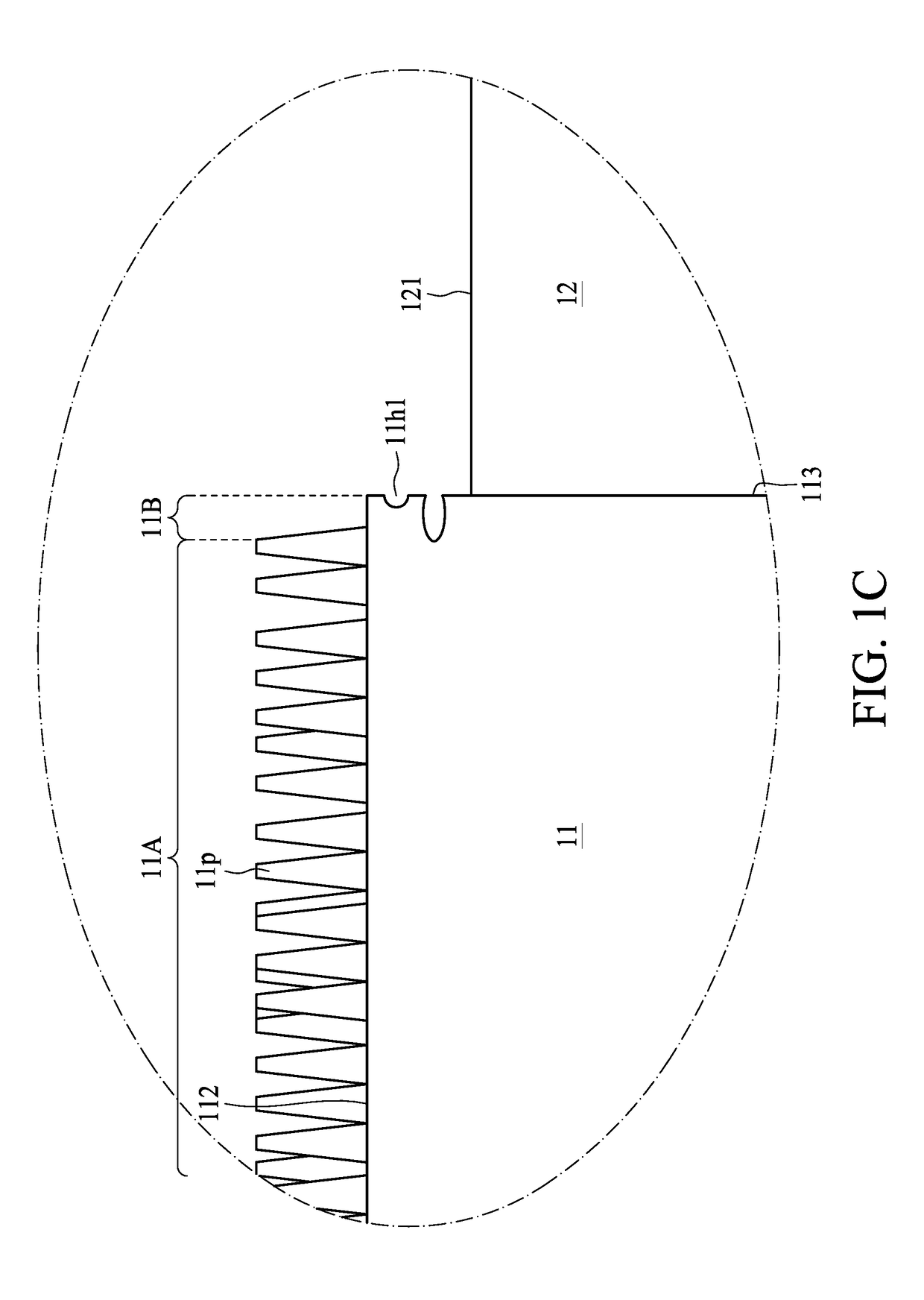
[0024]According to at least some embodiments of the present disclosure, a semiconductor package device includes an electrical component (e.g., a die or a chip). A plurality of features in nanoscale (e.g., nanoscale pillars or holes) are disposed on a surface of the electrical component to improve heat dissipation of the semiconductor package device. The nanoscale features perform as heat dissipaters and replace a comparative heat sink, reducing manufacturing cost and an overall thickness of the semiconductor package device.
[0025]FIG. 1A illustrates a cross-sectional view of a semiconductor package device 1A in accordance with some embodiments of the present disclosure. The semiconductor package device 1A includes a substrate 10, an electrical component (e.g., a die or a chip) 11 and a package body 12.
[0026]The substrate 10 may be, for example, a printed circuit board (PCB), such as a paper-based copper foil laminate, a composite copper foil laminate, a polymer-impregnated glass-fibe...
PUM
 Abstract
Description
Claims
Application Information
 - Generate Ideas
- Intellectual Property
- Life Sciences
- Materials
- Tech Scout
- Unparalleled Data Quality
- Higher Quality Content
- 60% Fewer Hallucinations
Browse by: Latest US Patents, China's latest patents, Technical Efficacy Thesaurus, Application Domain, Technology Topic, Popular Technical Reports.
© 2025 PatSnap. All rights reserved.Legal|Privacy policy|Modern Slavery Act Transparency Statement|Sitemap|About US| Contact US: help@patsnap.com