
Photo resist as opaque aperture mask on multispectral filter arrays

Active Publication Date: 2019-03-14
MATERION
View PDF0 Cites 2 Cited by
  • Summary
  • Abstract
  • Description
  • Claims
  • Application Information

AI Technical Summary

Benefits of technology

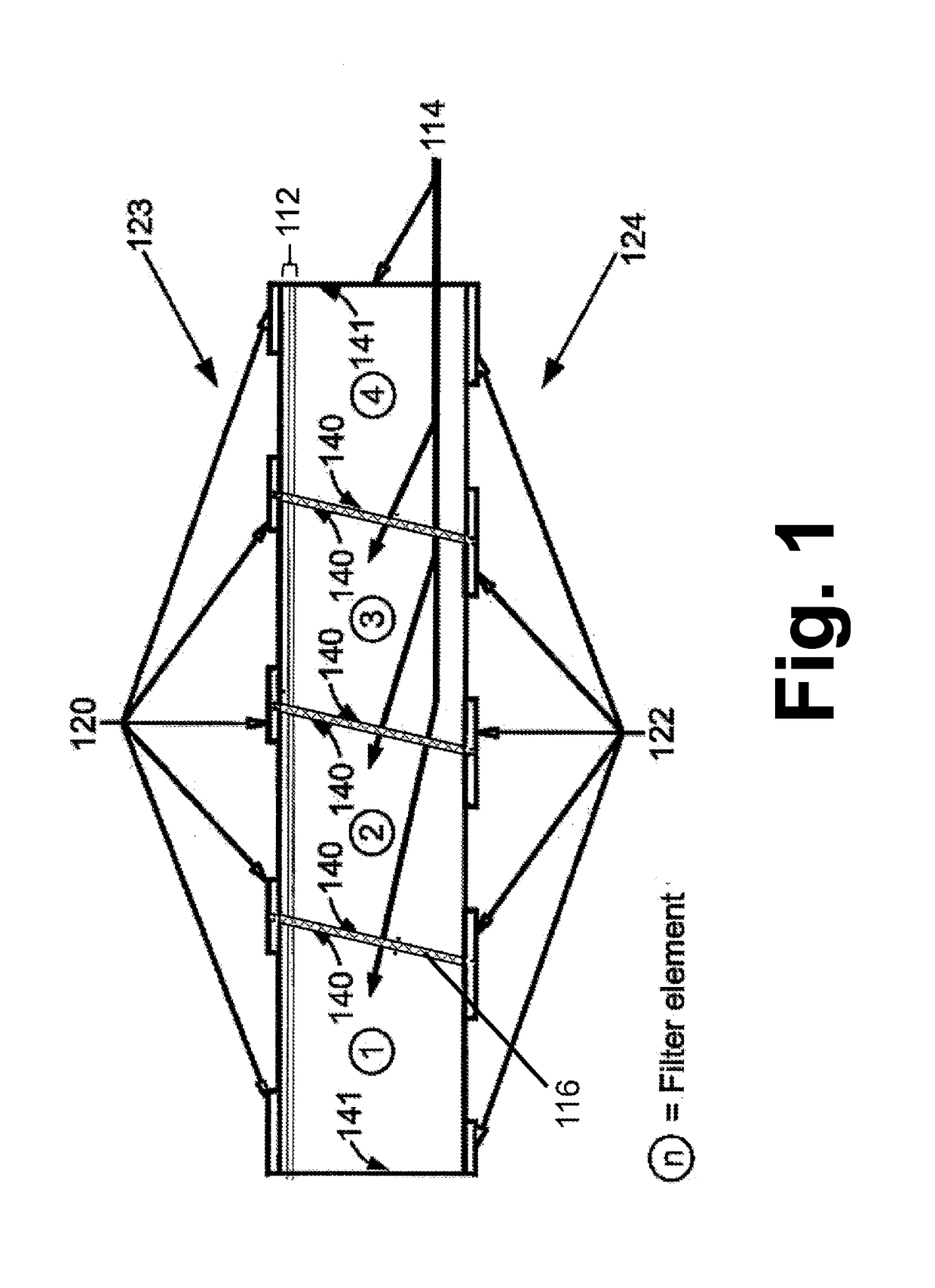
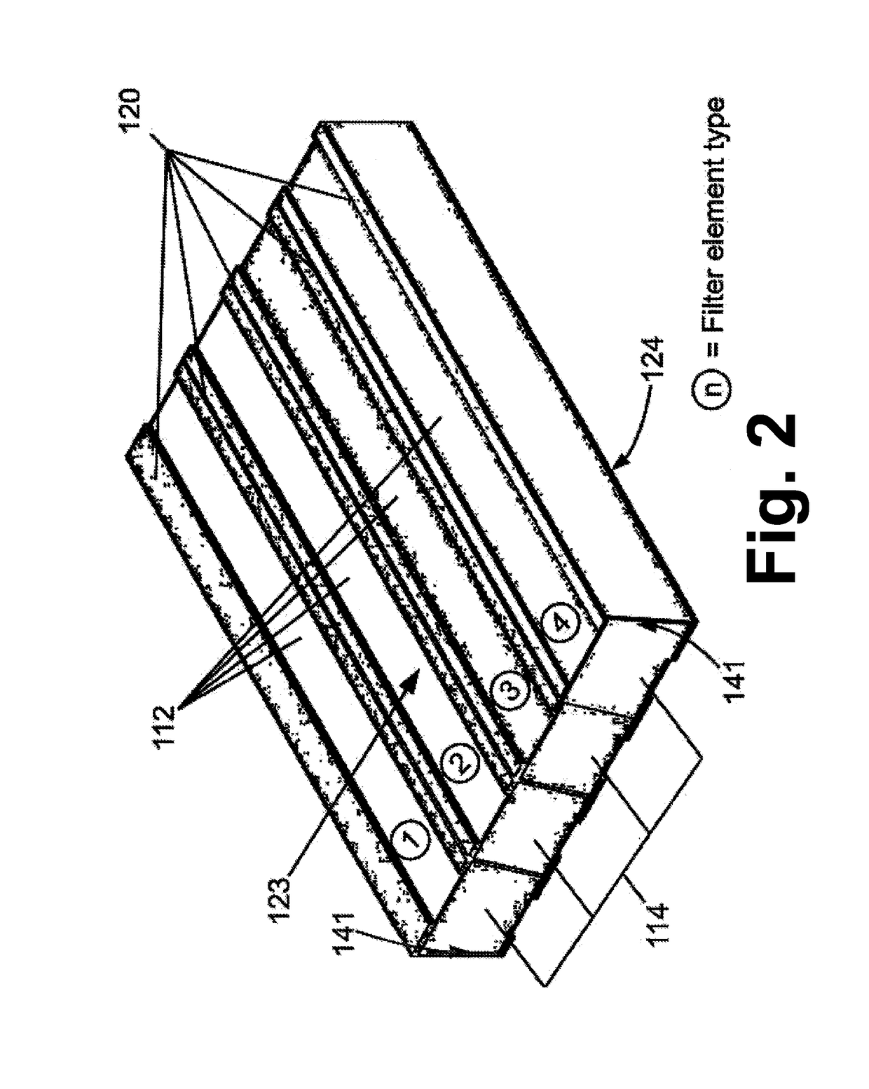
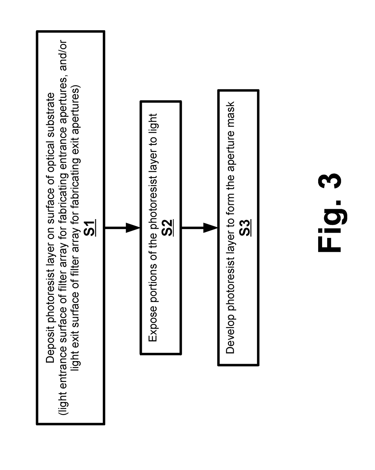
The patent describes methods and devices (such as optical filters and wafers) that have a mask made of photoresist printed on them. The mask can be used to create an aperture over a portion of the device. The mask can be deposited on both the light entrance and exit surfaces of the device, and can be made from a positive or negative photoresist. The device can also include an optical coating between the mask and the substrate. The presence of the mask can improve the performance and functionality of the device.

Problems solved by technology

However, it is difficult or impossible to vary the layer thicknesses across the substrate plate during layer deposition or by post deposition processing in a controlled manner in order to provide different pass bands or stop bands in different areas of the plate.
In the optical arts, if an image to be viewed is too bright, stray light can cause areas of bright light to bleed into adjoining dark areas and blur or eliminate the border between the bright and dark areas.
This can be particularly problematic when two bright areas are separated by a narrow dark area, because the irradiation can effectively cause the separating dark area to disappear.
This can result in too much glare existing for any significant detail to be seen.

Method used


Image

  • Photo resist as opaque aperture mask on multispectral filter arrays
  • Photo resist as opaque aperture mask on multispectral filter arrays
  • Photo resist as opaque aperture mask on multispectral filter arrays

Examples


Embodiment Construction

[0024]A more complete understanding of the components, processes and apparatuses disclosed herein can be obtained by reference to the accompanying drawings. These figures are merely schematic representations based on convenience and the ease of demonstrating the present disclosure, and are, therefore, not intended to indicate relative size and dimensions of the devices or components thereof and / or to define or limit the scope of the exemplary embodiments.

[0025]Although specific terms are used in the following description for the sake of clarity, these terms are intended to refer only to the particular structure of the embodiments selected for illustration in the drawings, and are not intended to define or limit the scope of the disclosure. In the drawings and the following description below, it is to be understood that like numeric designations refer to components of like function.

[0026]Unless otherwise defined, all technical and scientific terms used herein have the same meaning as...


PUM


Abstract

An apparatus (e.g., a multi-spectral optical filter array, an optical wafer, an optical component) has an aperture mask printed directly thereon, the aperture mask including a positive or negative photoresist. The apparatus includes a substrate having the aperture mask printed on at least one of a light entrance surface or a light exit surface of the substrate so as to provide an aperture over a portion of the substrate. The photoresist from which the aperture mask is formed is photo-definable or non-photo-definable, and is deposited / printed to form the aperture mask on the substrate.

Description

[0001]This application claims the benefit of U.S. Provisional Application No. 62 / 557,909 filed Sep. 13, 2017 and titled “PHOTO RESIST AS OPAQUE APERTURE MASK ON MULTISPECTRAL FILTER ARRAYS”. U.S. Provisional Application No. 62 / 557,909 filed Sep. 13, 2017 and titled “PHOTO RESIST AS OPAQUE APERTURE MASK ON MULTISPECTRAL FILTER ARRAYS” is hereby incorporated by reference in its entirety into the specification of this application.BACKGROUND[0002]The present disclosure relates to the optical arts, optical filter arts, spectrographic arts, and related arts.[0003]Optical filters with high spectral selectivity can be manufactured using a stack of layers, with alternating layers of two (or more) constituent materials having different refractive index values. Such filters are sometimes called interference filters, and can be designed to provide a designed pass-band, stop-band, high-pass, or low-pass output. For pass-band filters, the width of the pass band can typically be made as narrow as ...

Claims


Application Information

Patent Timeline
IPC IPC(8): G02B5/20G03F7/20G03F7/039G03F7/038G03F7/00
CPCG02B5/201G03F7/70308G03F7/0392G03F7/0382G03F7/0015
Inventor DOWNING, KEVIN R.
Owner MATERION
Learn More