

Connection structure of semiconductor device and manufacturing method thereof
- Summary
- Abstract
- Description
- Claims
- Application Information
AI Technical Summary
Benefits of technology
Problems solved by technology
Method used
Image

Examples
Embodiment Construction
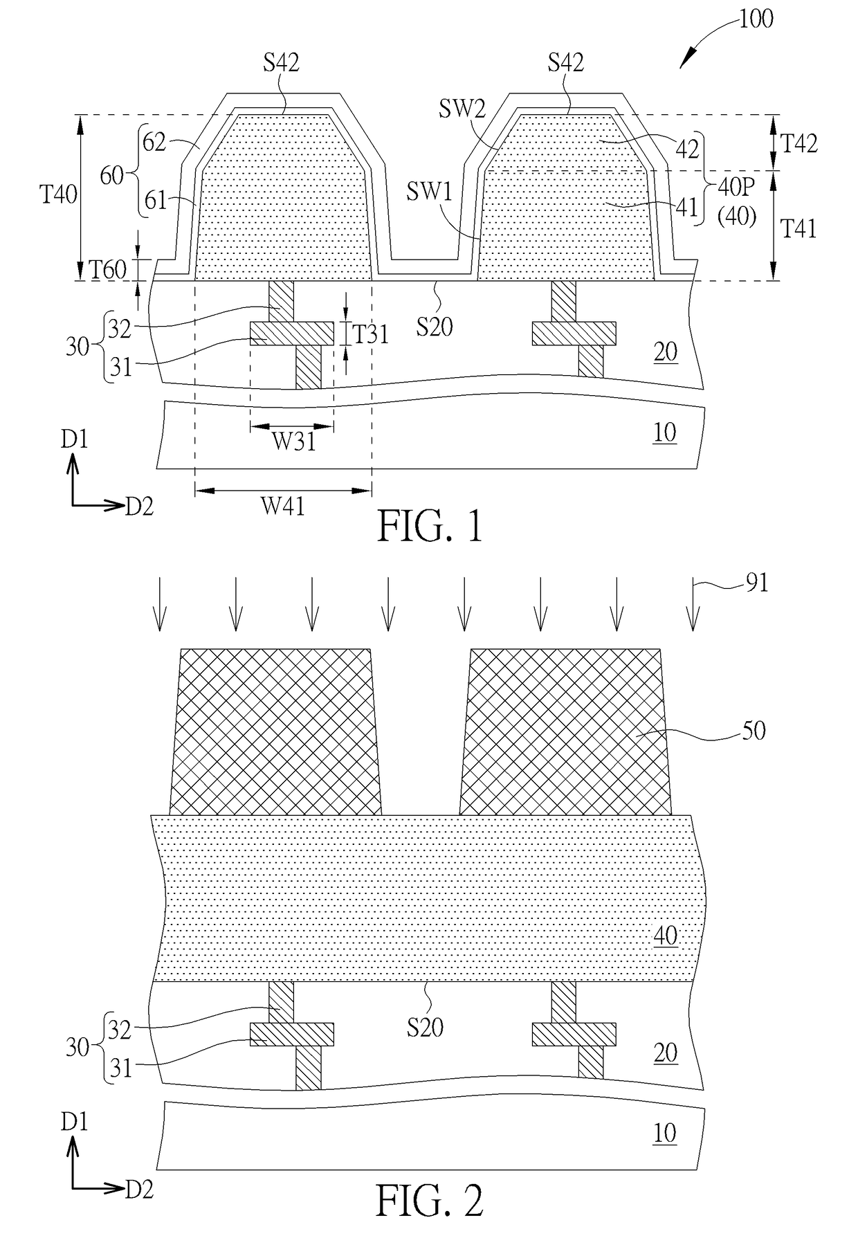
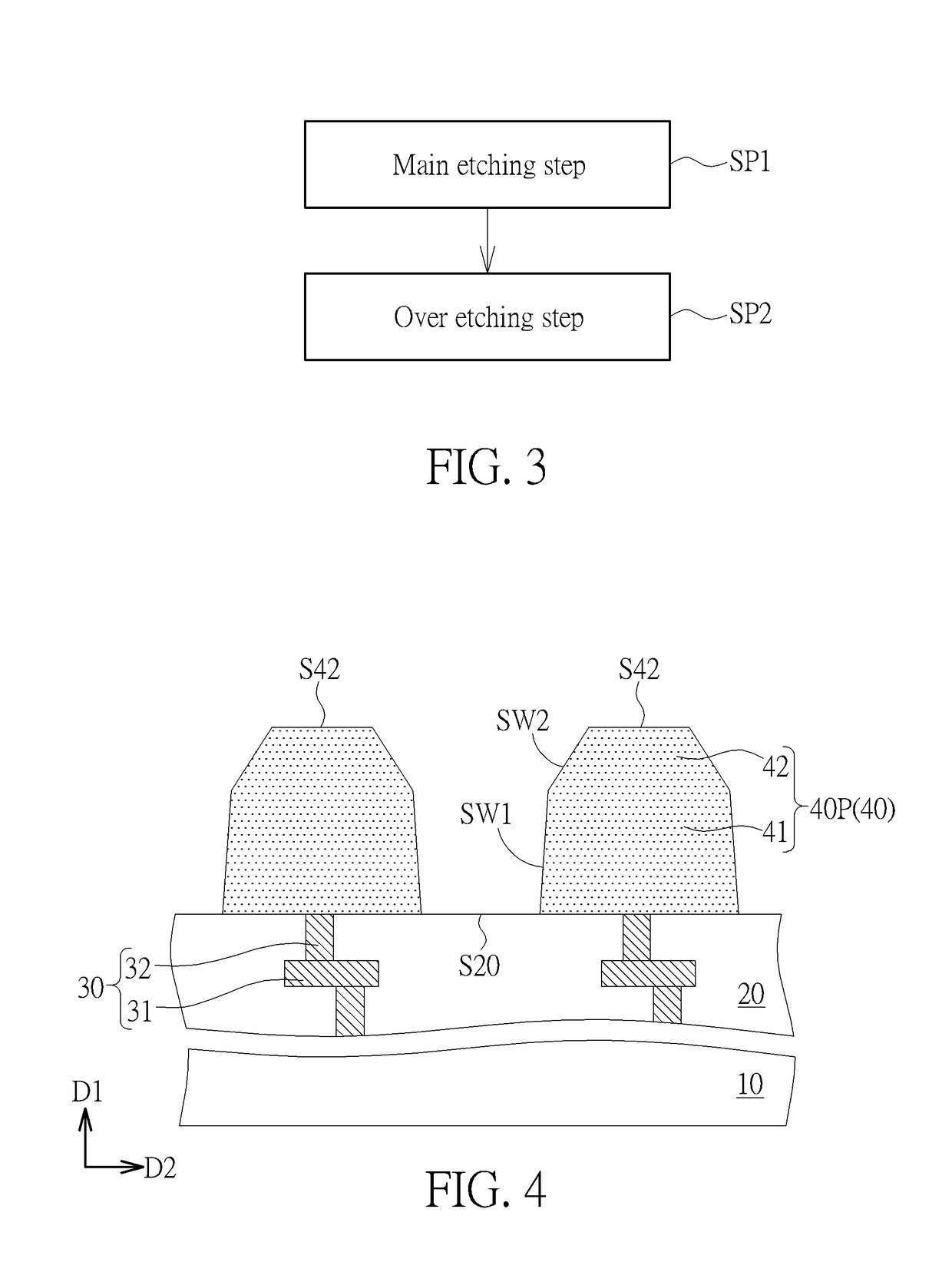
[0012]Please refer to FIG. 1. FIG. 1 is a schematic drawing illustrating a connection structure of a semiconductor device according to an embodiment of the present invention. As shown in FIG. 1, the connection structure 100 of the semiconductor device includes an interlayer dielectric (ILD) 20, a top metal structure 40P, and a passivation layer 60. The interlayer dielectric 20 is disposed on a substrate 10. The substrate may include a semiconductor substrate such as a silicon substrate, a silicon germanium substrate, or a silicon-on-insulator (SOI) substrate, but not limited thereto. In some embodiments, semiconductor units (such as silicon based field effect transistors, not shown) may be formed on the substrate 10 before the step of forming the interlayer dielectric 20, and the interlayer dielectric 20 may be formed after the step of forming the semiconductor units and cover the semiconductor units, but not limited thereto. The material of the interlayer dielectric 20 may include ...
PUM
 Abstract
Description
Claims
Application Information