Electronic component, diaphragm, and electronic device

Active Publication Date: 2019-03-28
MURATA MFG CO LTD
View PDF0 Cites 5 Cited by
  • Summary
  • Abstract
  • Description
  • Claims
  • Application Information

AI Technical Summary

Benefits of technology

[0007]Preferred embodiments of the present invention provide electronic components in each of which the sufficient bonding strength to the mounting substrate is easily be secured in mounting the electronic comp

Problems solved by technology

However, in the electronic component having the above configuration, when a large mounting electrode is formed on the mounting surface, this mounting electrode may interfere with a magnetic flux passing through the coil.
However, when such a mounting electrode is bonded to a conductor pattern formed on the mounting substrate with a conductive bonding material, such as solder interposed therebetween, there is a risk that sufficient bonding strength to the mounting

Method used


Image

  • Electronic component, diaphragm, and electronic device
  • Electronic component, diaphragm, and electronic device
  • Electronic component, diaphragm, and electronic device

Examples


first preferred embodiment

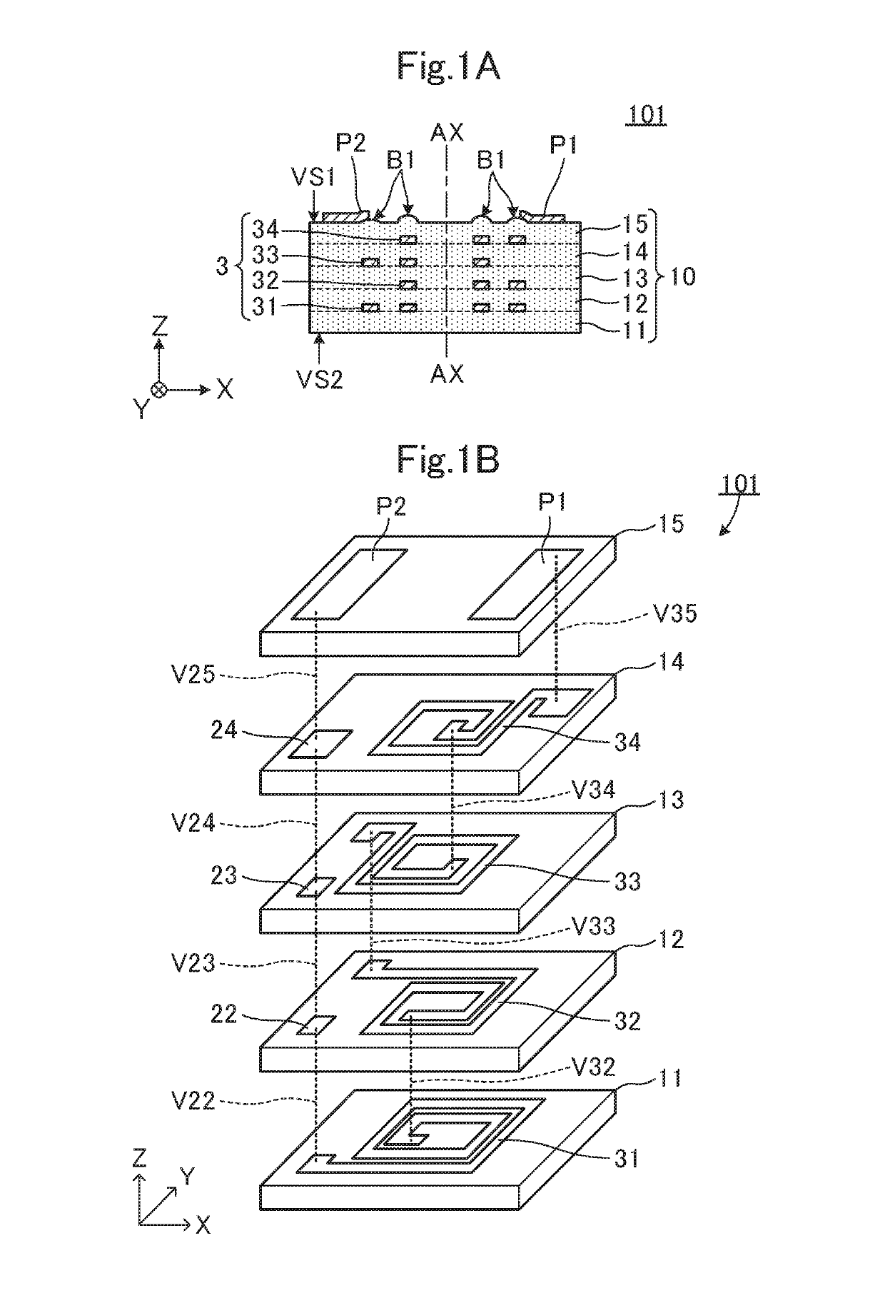
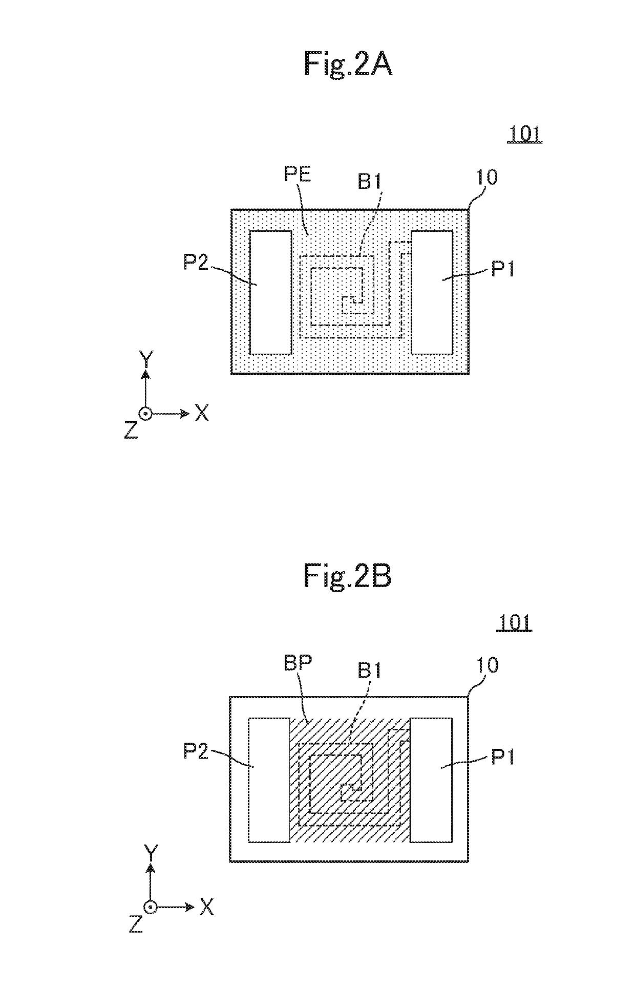
[0059]FIG. 1A is a sectional view of an electronic component 101 according to a first preferred embodiment, and FIG. 1B is an exploded perspective view of the electronic component 101. FIG. 2A is a plan view of the electronic component 101 and illustrates an electrode non-forming portion PE, and FIG. 2B is a plan view of the electronic component 101 and illustrates a bonding portion BP including a projection B1 of a first main surface VS1. In FIG. 1A, a thickness of each component is illustrated in an exaggerated manner. The same is true for sectional views in the following preferred embodiments. In FIG. 2A, the electrode non-forming portion PE is indicated by a dot pattern in order to easily understand the structure. In FIG. 2B, the bonding portion BP including the projection B1 of the first main surface VS1 is indicated by hatching.

[0060]The electronic component is an element mounted on a mounting substrate or other suitable substrate using a conductive bonding material and an ins...

second preferred embodiment

[0099]An example in which the entire electrode non-forming portion is bonded to the mounting substrate with the insulating bonding material interposed therebetween will be described in a second preferred embodiment of the present invention.

[0100]FIG. 6A is a plan view of an electronic component 102 according to the second preferred embodiment of the present invention and illustrates the bonding portion BP, and FIG. 6B is a sectional view illustrating a main portion of an electronic device 302 of the second preferred embodiment. In FIG. 6A, the bonding portion BP is indicated by hatching in order to easily understand the structure.

[0101]The electronic component 102 differs from the electronic component 101 of the first preferred embodiment in that the bonding portion BP is the entire electrode non-forming portion PE. In other words, the bonding portion BP and the electrode non-forming portion PE are matched with each other. Other configurations are identical or substantially identica...

third preferred embodiment

[0104]An example in which a portion of a coil is provided on the surface of the insulating base material is illustrated in a third preferred embodiment of the present invention.

[0105]FIG. 7A is a sectional view of an electronic component 103 of the third preferred embodiment, and FIG. 7B is an exploded perspective view of the electronic component 103.

[0106]The electronic component 103 includes an insulating base material 10B including the first main surface VS1 and the second main surface VS2 opposite to the first main surface VS1, a coil 3A (to be described in detail later), the mounting electrodes P1, P2 provided on the first main surface VS1, the projection B1, and a protective layer 1.

[0107]The insulating base material 10B has a rectangular or substantially rectangular parallelepiped shape preferably made of a thermoplastic resin, for example, in which a longitudinal direction is matched with the X-axis direction. As illustrated in FIG. 7B, the insulating base material 10B is fo...


PUM


Abstract

An electronic component includes an insulating base material including insulating base material layers, a first main surface that is a mounting surface, a coil, mounting electrodes provided on the first main surface, and a projection. The coil includes coil conductors provided on the insulating base material layers and a winding axis in a laminating direction of the insulating base material layers. The projection is provided in an electrode non-forming portion of the first main surface, the electrode non-forming portion including no mounting electrodes therein, and provided along the coil conductors in planar view of the first main surface.

Description

CROSS REFERENCE TO RELATED APPLICATIONS[0001]This application claims the benefit of priority to Japanese Patent Application No. 2016-113494 filed on Jun. 7, 2016, Japanese Patent Application No. 2016-153421 filed on Aug. 4, 2016, Japanese Patent Application No. 2016-216983 filed on Nov. 7, 2016, and Japanese Patent Application No. 2017-006700 filed on Jan. 18, 2017 and is a Continuation Application of PCT Application No. PCT / JP2017 / 020188 filed on May 31, 2017. The entire contents of these applications are hereby incorporated herein by reference.BACKGROUND OF THE INVENTION1. Field of the Invention[0002]The present invention relates to an electronic component, particularly to an electronic component in which a coil is provided on an insulating base material, a diaphragm including the electronic component, and an electronic device including the electronic component or the diaphragm.2. Description of the Related Art[0003]Various electronic components, in which the coil is formed on the...

Claims


Application Information

Patent Timeline
IPC IPC(8): H01F7/20H01F27/28H01F27/29H01F27/32H05K1/18H04R9/00H04R7/00
CPCH01F7/20H01F27/2804H01F27/29H01F27/323H05K1/181H04R9/00H04R7/00H01F2007/068H01F2027/2809H05K2201/10083B06B1/04H01F17/0013H01F27/292H01F41/041H01F2017/004H04R9/046H05K3/305H05K3/3436H05K2201/1003H05K2201/10992Y02P70/50
Inventor ITO, SHINGOGOUCHI, NAOKITAKEUCHI, KOSUKE
Owner MURATA MFG CO LTD
Why Eureka
Try Eureka