
Anti-hacking mechanisms for flash memory device

Active Publication Date: 2019-04-18
SILICON STORATE TECH INC
View PDF15 Cites 16 Cited by
  • Summary
  • Abstract
  • Description
  • Claims
  • Application Information

AI Technical Summary

Benefits of technology

This patent discusses various ways to enhance the security and prevent hacking of a flash memory device. These methods include using fault detection circuits, address scrambling, dummy arrays, password protection, and improved manufacturing techniques. The goal is to make it difficult for malicious individuals to hack the flash memory chip and gain access to the data stored within it.

Problems solved by technology

These measures, however, do not prevent someone from disassembling the phone and retrieving data directly from non-volatile storage such as from a flash memory device.
To date, the security measures available for flash memory devices have been extremely limited.

Method used


Image

  • Anti-hacking mechanisms for flash memory device
  • Anti-hacking mechanisms for flash memory device
  • Anti-hacking mechanisms for flash memory device

Examples


Embodiment Construction

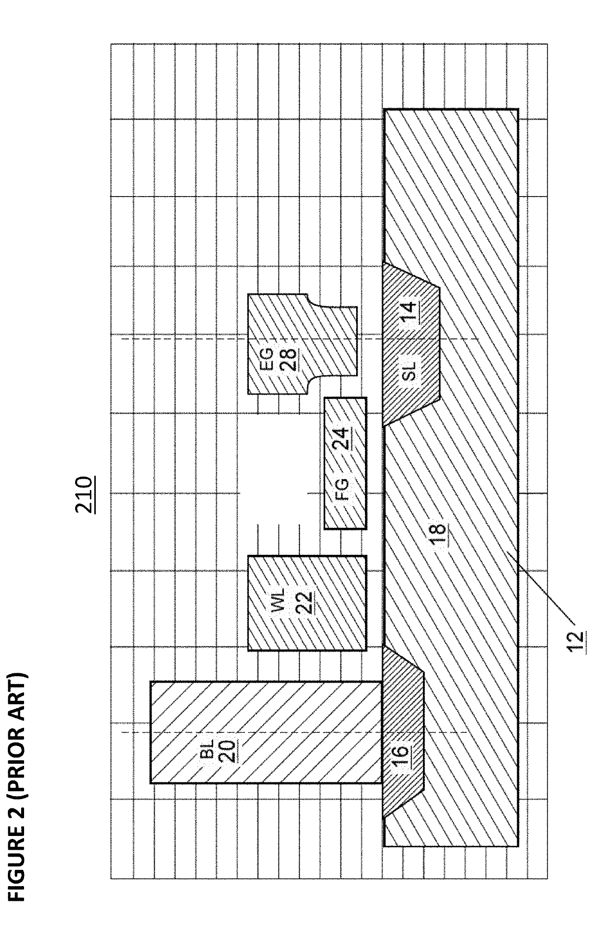
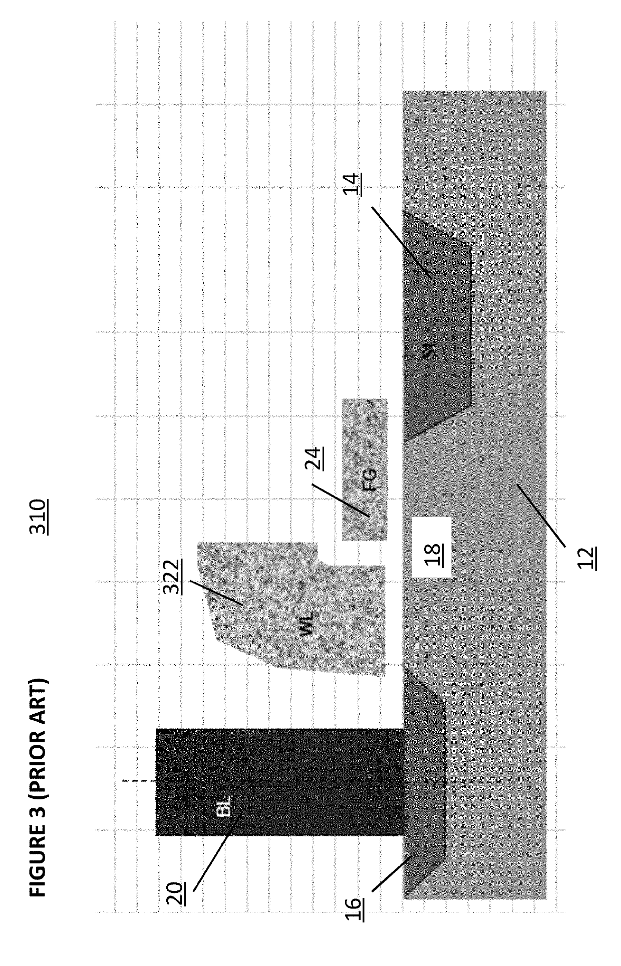
[0043]FIG. 4 depicts an embodiment of a flash memory system comprising the security enhancements described herein. Die 400 comprises: memory arrays 401, 402, 403, and 404 for storing data, each memory array optionally utilizing memory cell 4 as in FIG. 1, memory cell 24 as in FIG. 2, memory cell 34 as in FIG. 3, or other known types of memory cells; row decoder circuits 405, 406, 407, and 408 used to access the row in memory arrays 401, 402, 403, and 404, respectively, to be read from or written to; column decoder circuits 409, 410, 411, and 412 used to access the column in memory arrays 401, 402, 403, and 404, respectively, to be read from or written to; sensing circuit 413 used to read data from memory arrays 401 and 403 and sensing circuit 414 used to read data from memory arrays 402 and 404; analog, chip fault detection (CFD), and physically unclonable function (PUF) circuits 450; logic and logic fault detection (LFD) circuits 451 for providing various control functions, such as...


PUM


Abstract

Multiple embodiments are disclosed for enhancing security and preventing hacking of a flash memory device. The embodiments prevent malicious actors from hacking a flash memory chip to obtain data that is stored within the chip. The embodiments include the use of fault detection circuits, address scrambling, dummy arrays, password protection, improved manufacturing techniques, and other mechanisms.

Description

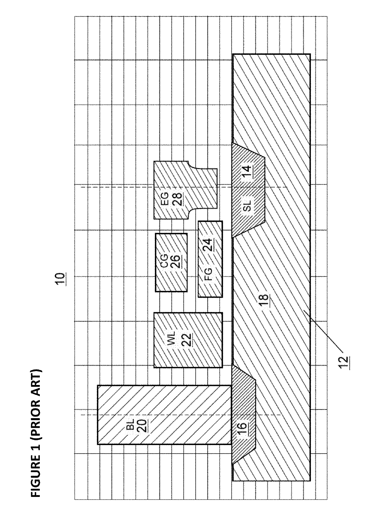
TECHNICAL FIELD[0001]A multitude of mechanisms are disclosed for enhancing security and preventing hacking of a flash memory device.BACKGROUND OF THE INVENTION[0002]Non-volatile memory cells are well known in the art. One prior art non-volatile split gate memory cell 10, which contains five terminals, is shown in FIG. 1. Memory cell 10 comprises semiconductor substrate 12 of a first conductivity type, such as P type. Substrate 12 has a surface on which there is formed a first region 14 (also known as the source line SL) of a second conductivity type, such as N type. A second region 16 (also known as the drain line) also of N type is formed on the surface of substrate 12. Between the first region 14 and the second region 16 is channel region 18. Bit line BL 20 is connected to the second region 16. Word line WL 22 is positioned above a first portion of the channel region 18 and is insulated therefrom. Word line 22 has little or no overlap with the second region 16. Floating gate FG 24...

Claims


Application Information

Patent Timeline
IPC IPC(8): G06F3/06G06F11/07G11C16/08G11C16/26G11C16/34G11C16/10H01L29/423H01L23/00H01L21/78G11C16/04H01L27/11521
CPCG06F3/0622G06F11/073G06F11/0754G06F11/0793G06F3/0637G06F3/0679G11C16/08G11C16/26G11C16/3422G11C16/10H01L29/42328H01L23/576H01L21/78G11C16/0408H01L27/11521G11C16/22G11C7/06G11C29/12G06F21/79H10B41/35H10B41/41G11C16/0425G11C16/28G11C29/025G11C29/18G11C29/48G11C2029/0403G11C2029/1202G11C2029/1206G11C2029/4402Y04S40/20H04L9/3278G09C1/00G11C7/065H10B41/30
Inventor TRAN, HIEU VANTIWARI, VIPINDO, NHAN
Owner SILICON STORATE TECH INC
Learn More