Transfer system for flipping and multiple checking of electronic devices

a technology of electronic devices and transfer systems, applied in the direction of electrical equipment, semiconductor/solid-state device manufacturing, conveying parts, etc., can solve the problems of increasing the likelihood of packages being dropped and/or damaged, system is impractical for industrial use, and the device is only capable of flipping a limited number of units, so as to increase the inspection time of electronic devices

Active Publication Date: 2019-05-09
MIT SEMICON (TIAN JIN) CO LTD
View PDF3 Cites 7 Cited by
  • Summary
  • Abstract
  • Description
  • Claims
  • Application Information

AI Technical Summary

Benefits of technology

[0023]In another aspect, the first reflecting device is configured to increase an inspection time of the electronic devices when picking the electronic devices from the wafer table.

Problems solved by technology

Conventional flipping mechanisms increase the frequency by which the semiconductor packages are picked and placed, which increases the likelihood that packages are dropped and / or damaged.
This system is impractical for industrial use because it has only one pickup element and relies on a time-consuming sequential method process.
The device of FIG. 2 uses only two vacuum pipettes to flip the chip, hence the device is only capable of flipping a limited number of units per hour (UPH).
Because the transfer apparatus uses a vertical wafer table, chips are prone to falling from the wafer and becoming damaged.
However, because there is only one vertical flipper, it is only possible to have one check station.

Method used


Image

  • Transfer system for flipping and multiple checking of electronic devices
  • Transfer system for flipping and multiple checking of electronic devices
  • Transfer system for flipping and multiple checking of electronic devices

Examples


Embodiment Construction

[0039]The particular values and configurations discussed in the following non-limiting examples can be varied, are cited merely to illustrate at least one embodiment, and are not intended to limit the scope thereof.

[0040]Without intent to further limit the scope of the disclosure, examples of instruments, apparatus, methods and their related results according to the embodiments of the present disclosure are given below. Note that titles or subtitles may be used in the examples for convenience of a reader, which in no way should limit the scope of the disclosure. Unless otherwise defined, all technical and scientific terms used herein have the same meaning as commonly understood by one of ordinary skill in the art to which this disclosure pertains. In the case of conflict, the present document, including definitions, will control.

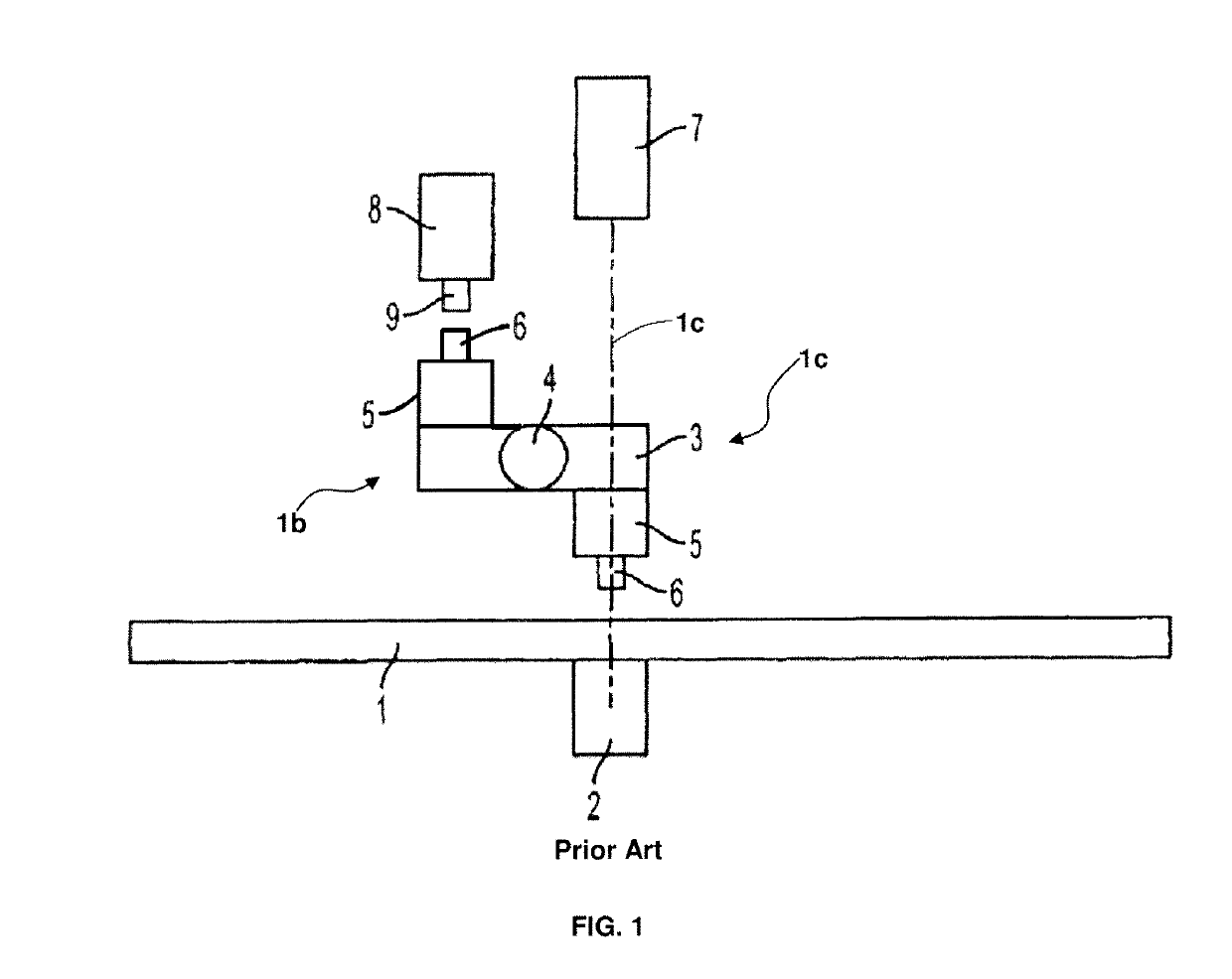
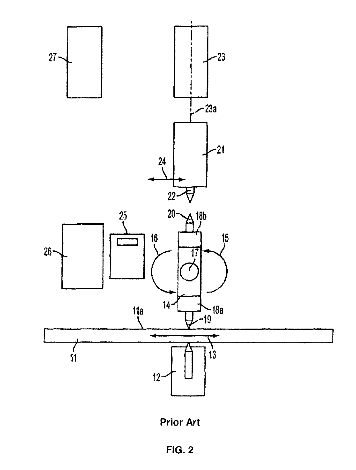
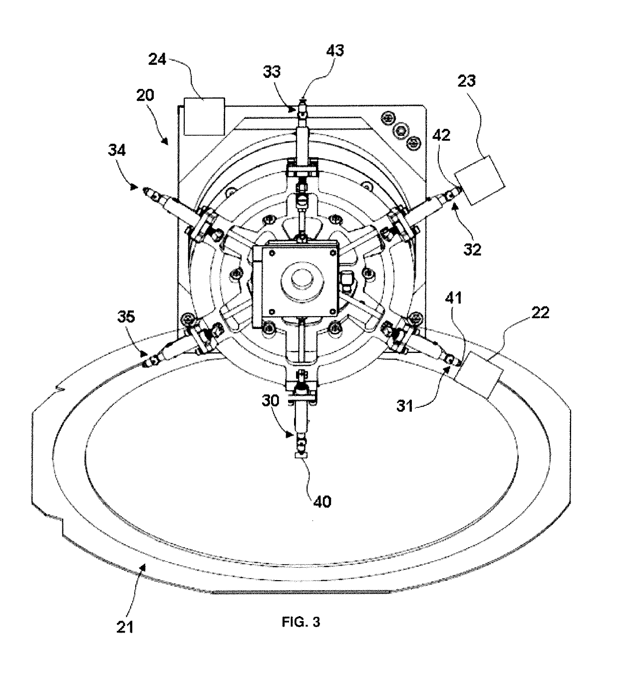
[0041]The term “ball grid array” or “BGA” as used herein, refers to type of surface-mount packaging (a chip carrier) used for integrated circuits.

[0042]The ...


PUM


Abstract

The present invention includes a transfer system for flipping and checking electronic devices. A first rotary device has a plurality of transfer heads configured to pick electronic devices from a wafer table and place the electronic devices on a transfer head of a second rotary device. Check stations can be positioned around the first and second rotary devices and configured to inspect or check the electronic devices during the flipping process. The transfer system can further include an imaging device to inspect the accuracy of picking and placing of the electronic devices during the flipping process. The wafer table and the first rotary device are inclined to increase the operation space. The system accurately picks, flips and transfers chips at a high operation speed.

Description

FIELD OF THE INVENTION[0001]The following description relates generally to a transfer system for transferring and changing the orientation of electronic devices such as semiconductor chips, and more specifically, to a system for transferring and flipping chips that provides additional operation space and greater efficacy than conventional systems.BACKGROUND[0002]Semiconductor device fabrication is the process used to create the integrated circuits that are present in everyday electrical and electronic devices. In typical semiconductor fabrication, integrated circuits (“ICs” or “chips”) are built in large quantities on a single large wafer of semiconductor material, typically silicon. The individual chips are patterned with small pads of metal near their edges that serve as connections to a mechanical carrier. The chips are then cut out of the wafer and attached to carriers, typically via wire bonding such as thermosonic bonding. The wires used in the wire bonding eventually lead to ...

Claims


Application Information

Patent Timeline
Patent Type & Authority Applications(United States)
IPC IPC(8): H01L21/67H01L21/683H01L21/68B65G47/84
CPCH01L21/67144H01L21/6838H01L21/67259H01L21/681B65G47/848H01L21/67742
Inventor NEO, SIONG HUATKWONG, KIM MONELIM, KOK YEOWMAO, ZHI QIANG
Owner MIT SEMICON (TIAN JIN) CO LTD
Why Eureka
Try Eureka