Supercharge Your Innovation With Domain-Expert AI Agents!

Multi-Phase Half Bridge Driver Package and Methods of Manufacture

a driver package and driver technology, applied in the direction of pulse technique, electronic switching, basic electric elements, etc., can solve the problems of large footprint, large footprint, and inability to provide built-in cooling features, and achieve the effect of reducing the number of components

Active Publication Date: 2019-05-30
INFINEON TECH AG
View PDF6 Cites 1 Cited by
  • Summary
  • Abstract
  • Description
  • Claims
  • Application Information

AI Technical Summary

Benefits of technology

The patent describes a semiconductor package that includes multiple half bridges, each containing a power transistor die and a metal lead. The half bridges are embedded in a mold compound. The package also includes a controller die and bond wire connections between the controller die and the power transistor dies. The technical effects of this design include improved cooling, reduced inductance, and improved efficiency. Additionally, the package design allows for more flexibility in routing and placement of power transistor dies, making it easier to create custom configurations.

Problems solved by technology

The integration of multiple power transistors and a microcontroller in a small and thin package presents several challenges.
), and consume significant power (e.g. up to 500 W).
Such a solution has a large footprint and provides no built-in cooling features.
Such a conventional board-based implementation of a multi-phase half bridge driver also suffers from voltage spikes and higher levels of EMI (electromagnetic interference), due to high inductance connections between the dies and the board.

Method used


Image

  • Multi-Phase Half Bridge Driver Package and Methods of Manufacture
  • Multi-Phase Half Bridge Driver Package and Methods of Manufacture
  • Multi-Phase Half Bridge Driver Package and Methods of Manufacture

Examples


Embodiment Construction

[0018]Embodiments described herein provide an integrated package solution for multi-phase half bridge drivers that has a small footprint, good heat dissipation characteristics and low inductance compared to board-based solutions. The integrated package solution described herein also has reduced voltage spikes and less EMI, due to lower inductance connections to the package. Also, the integrated package solution yields a system-level cost savings due to reduced input filtering requirements.

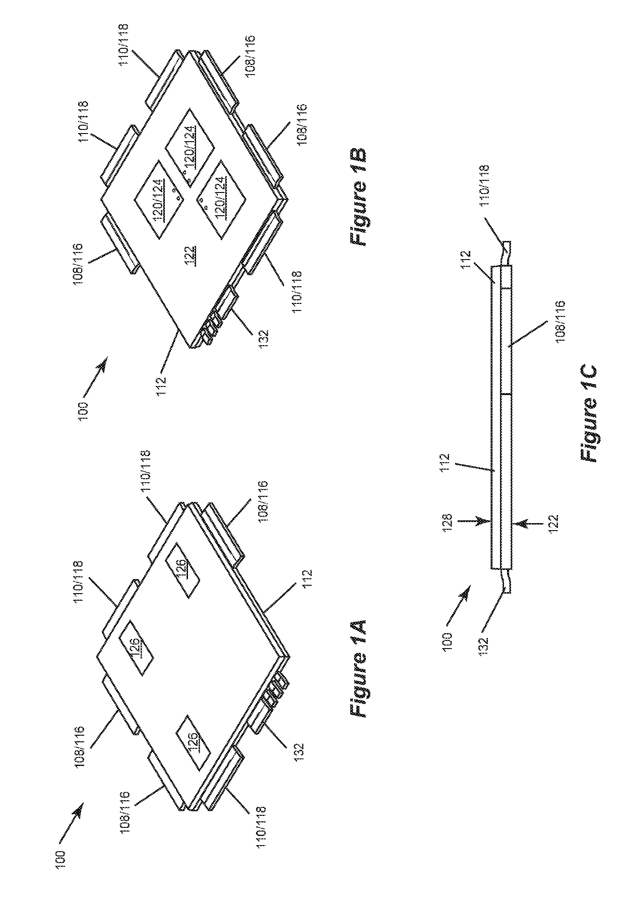
[0019]FIG. 1A illustrates a top perspective view of an embodiment of a multi-phase half bridge driver package 100.

[0020]FIG. 1B illustrates a bottom perspective view of the multi-phase half bridge driver package 100.

[0021]FIG. 1C illustrates a side perspective view of the multi-phase half bridge driver package 100.

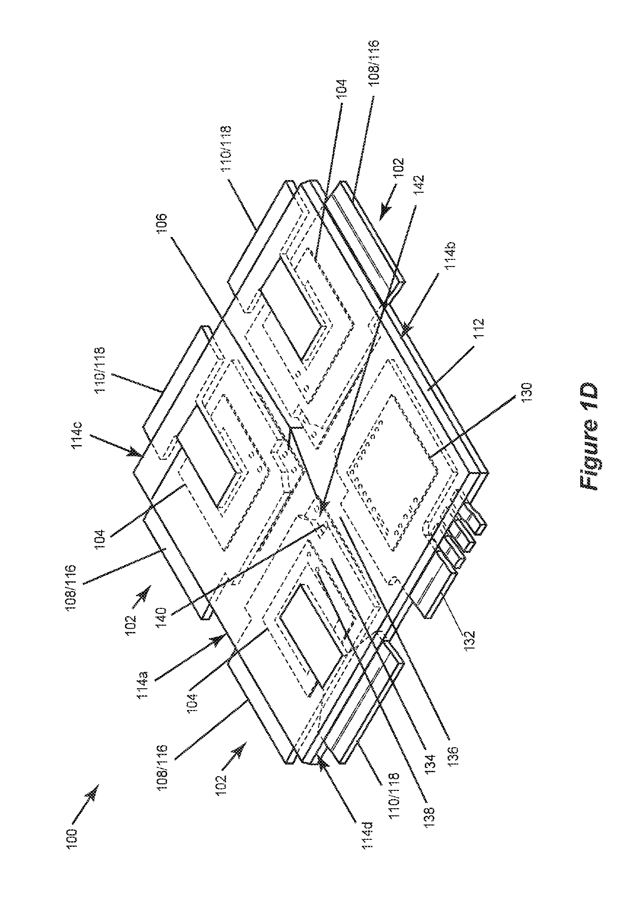
[0022]FIG. 1D illustrates the same top perspective view in FIG. 1A, but with the mold compound removed in certain areas to show interior components of the package 100.

[0023]The multi-phas...


PUM


Abstract

A semiconductor package includes a plurality of half bridge assemblies each including a metal lead, a first power transistor die attached to a first side of the metal lead, and a second power transistor die disposed under the first power transistor die and attached to a second side of the metal lead opposite the first side. Each metal lead has a notch which exposes one or more bond pads at a side of the second power transistor die attached to the metal lead. The semiconductor package also includes a controller die configured to control the power transistor dies. Each power transistor die, each metal lead and the controller die are embedded in a mold compound. Bond wire connections are provided between the controller die and the one or more bond pads at the side of each second power transistor die exposed by the notch in the corresponding metal lead.

Description

BACKGROUND[0001]The integration of multiple power transistors and a microcontroller in a small and thin package presents several challenges. For example, multi-phase brushless DC motors require high current (e.g. between 70 A to 120 A), operate at high temperature (e.g. above 150° C.), and consume significant power (e.g. up to 500 W). A half bridge driver for such an application generates significant heat that must be dissipated by the package. Conventional multi-phase half bridge drivers are implemented by attaching the half bridge power transistor dies and the corresponding controller die to a printed circuit board (PCB). Such a solution has a large footprint and provides no built-in cooling features. Such a conventional board-based implementation of a multi-phase half bridge driver also suffers from voltage spikes and higher levels of EMI (electromagnetic interference), due to high inductance connections between the dies and the board.[0002]Hence, there is a need for an improved ...

Claims


Application Information

Patent Timeline
Patent Type & Authority Applications(United States)
IPC IPC(8): H01L23/495H03K17/687H01L23/31H01L21/48H01L21/56
CPCH01L23/49575H03K17/6871H01L23/3114H01L23/4951H01L23/4952H01L23/49537H01L23/49562H01L23/49568H01L21/4803H01L21/4825H01L21/565H02P27/04H02M1/088H01L23/49541H01L23/3107H01L2224/48471H01L2224/49109
Inventor CHIANG, CHAU FATTCHA, CHAN LAMKOO, WEI HANKUCHER, ANDREASLONG, THENG CHAO
Owner INFINEON TECH AG
Features
  • R&D
  • Intellectual Property
  • Life Sciences
  • Materials
  • Tech Scout
  • Unparalleled Data Quality
  • Higher Quality Content
  • 60% Fewer Hallucinations
Learn More