Top emission organic el element and manufacturing method thereof
- Summary
- Abstract
- Description
- Claims
- Application Information
AI Technical Summary
Benefits of technology
Problems solved by technology
Method used
Image
Examples
first embodiment
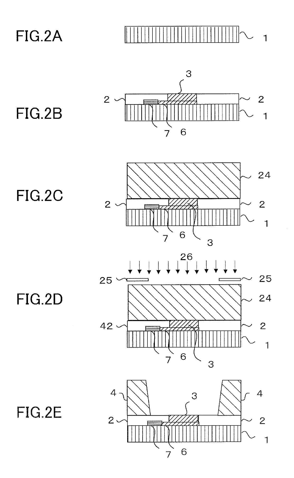
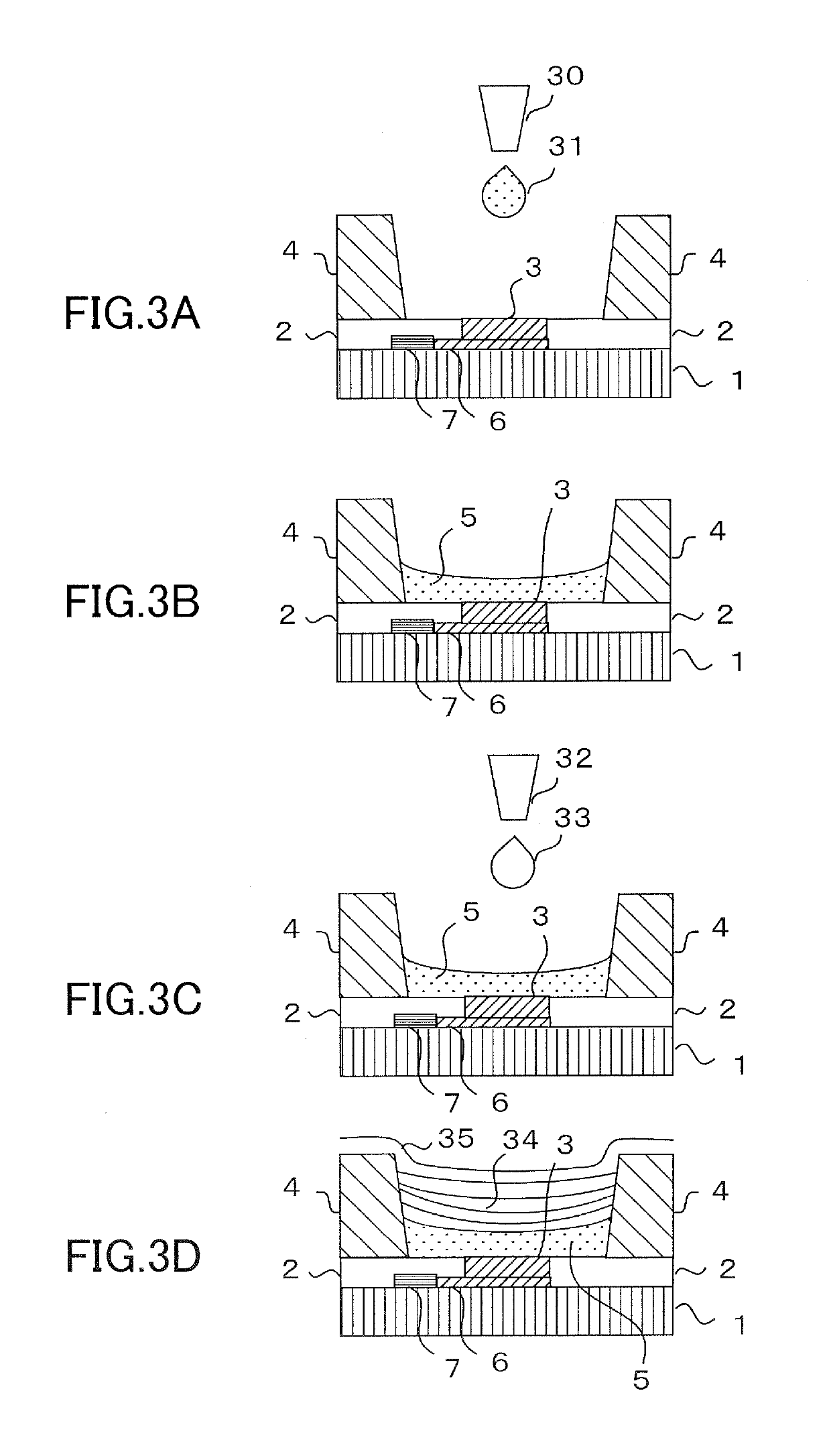
[0026]A top emission organic EL element and a manufacturing method thereof of a first embodiment of the present disclosure will be described with reference to the drawings.
Structure of Organic EL Element
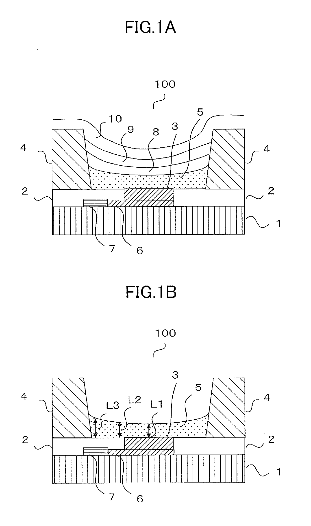
[0027]FIG. 1A is a schematic section view illustrating a configuration of an organic EL element 100 of the first embodiment of the present disclosure that is functionable as a pixel portion of a display panel or a light emitting portion of an illumination light source.
[0028]In FIG. 1A, the organic EL element 100 includes a substrate 1, an insulating layer 2, a plug 3 formed of a low contact angle material, a bank 4, a lower electrode 5, a connecting electrode 6, a TFT 7 which is a driving transistor, an light emitting layer 8, a hole injection layer 9 and an upper transparent electrode 10.
[0029]It is noted that a plurality of organic EL elements is arrayed one-dimensionally or two-dimensionally in a case where the organic EL element 100 of the present embodiment is used as a pixel of...
second embodiment
[0066]A top emission organic EL device and a manufacturing method thereof of a second embodiment of the present disclosure will be described below with reference to the drawings.
Structure of Organic EL Element
[0067]FIG. 4A is a schematic section view illustrating a configuration of an organic EL element of the second embodiment of the present disclosure functionable as a pixel portion of a display panel or a light emitting portion of an illumination light source.
[0068]In FIG. 4A, the organic EL element 400 includes a substrate 41, an insulating layer 42, a roughened surface region 43 formed at a center area of the insulating layer 42, a bank 44, a lower electrode 45, a light emitting layer 48, a hole injection layer 49 and an upper transparent electrode 50.
[0069]It is noted that a plurality of organic EL elements 400 is arrayed one-dimensionally or two-dimensionally in a case where the organic EL element 400 of the present embodiment is used as a pixel of a display panel or an eleme...
first example
[0083]A concrete example of the lower electrode of the first embodiment will be described. At first, a driving TFT is formed on a glass substrate for forming the element. Next, a contact hole is defined by photolithographic etching at a position corresponding to the center area in the region surrounded by the bank. Next, after filling the contact hole with Al by plating, an upper surface is planarized by CMP. An area of the plug is about one-tenth of an area of the region surrounded by the bank.
[0084]Still further, an ink repellent treatment is performed on the side surface of the bank so as to have a contact angle of 60 to 70° to the silver nanoparticle dispersed ink (manufactured by Daiken Chemical Co., Ltd. NAG series).
[0085]The contact angle to the ink of the upper surface of the center area, i.e., the plug, is 15° and the contact angle to the ink of the upper surface of the peripheral area, i.e., the insulating layer, is 70°.
[0086]In this condition, five droplets of 1 pl, i.e.,...
PUM
| Property | Measurement | Unit |
|---|---|---|
| Contact angle | aaaaa | aaaaa |
| Contact angle | aaaaa | aaaaa |
| Mean roughness | aaaaa | aaaaa |
Abstract
Description
Claims
Application Information


