Manufacture of optical elements by replication and corresponding replication tools and optical devices

a technology of optical elements and replication tools, applied in the field of microoptics, can solve the problems of limited precision of the dispensing process in which the replication material is applied between the replication tool and the substrate (typically on one or both of them), and achieve the effects of small contact angle, good asymmetries, and stable process conditions

Active Publication Date: 2017-03-30
AMS SENSORS SINGAPORE PTE LTD
View PDF1 Cites 2 Cited by
  • Summary
  • Abstract
  • Description
  • Claims
  • Application Information

AI Technical Summary

Benefits of technology

[0102]It turned out that particularly stable process conditions and good asymmetries can be achieved when materials are chosen such that a contact angle between the replication material (and thus the optical structure) and the first substrate surface is smaller than 40°, in particular smaller than 30°, more particularly smaller than 22°. It is furthermore possible to apply a coating to the first substrate surface with the effect of achieving a particularly small contact angle. Such a coating may be, e.g., an adhesion promoter for increasing an adhesion of the replication material to the (coated) first substrate surface. Contact angles of below 10° and more particularly below 5° can be achieved this way.

Problems solved by technology

Miniaturization and the need to provide more and more functionality per substrate area are important issues in micro-optics.
One reason for providing the additional amount of replication material (excess replication material) and the surrounding portion, respectively, is that a dispensing process in which the replication material is applied between the replication tool and the substrate (typically on one or both of them) has a limited precision.

Method used


Image

  • Manufacture of optical elements by replication and corresponding replication tools and optical devices
  • Manufacture of optical elements by replication and corresponding replication tools and optical devices
  • Manufacture of optical elements by replication and corresponding replication tools and optical devices

Examples


Embodiment Construction

[0131]The described embodiments are meant as examples and shall not limit the invention.

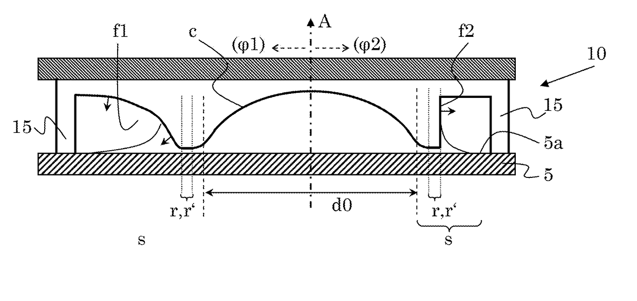
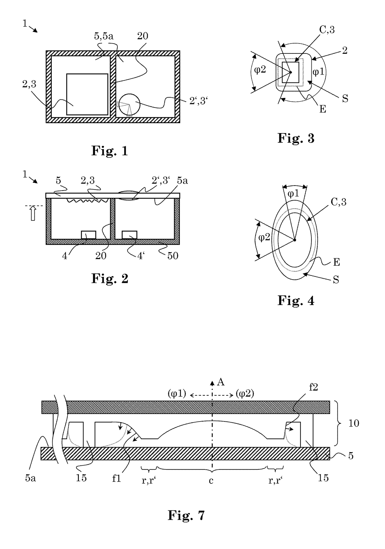
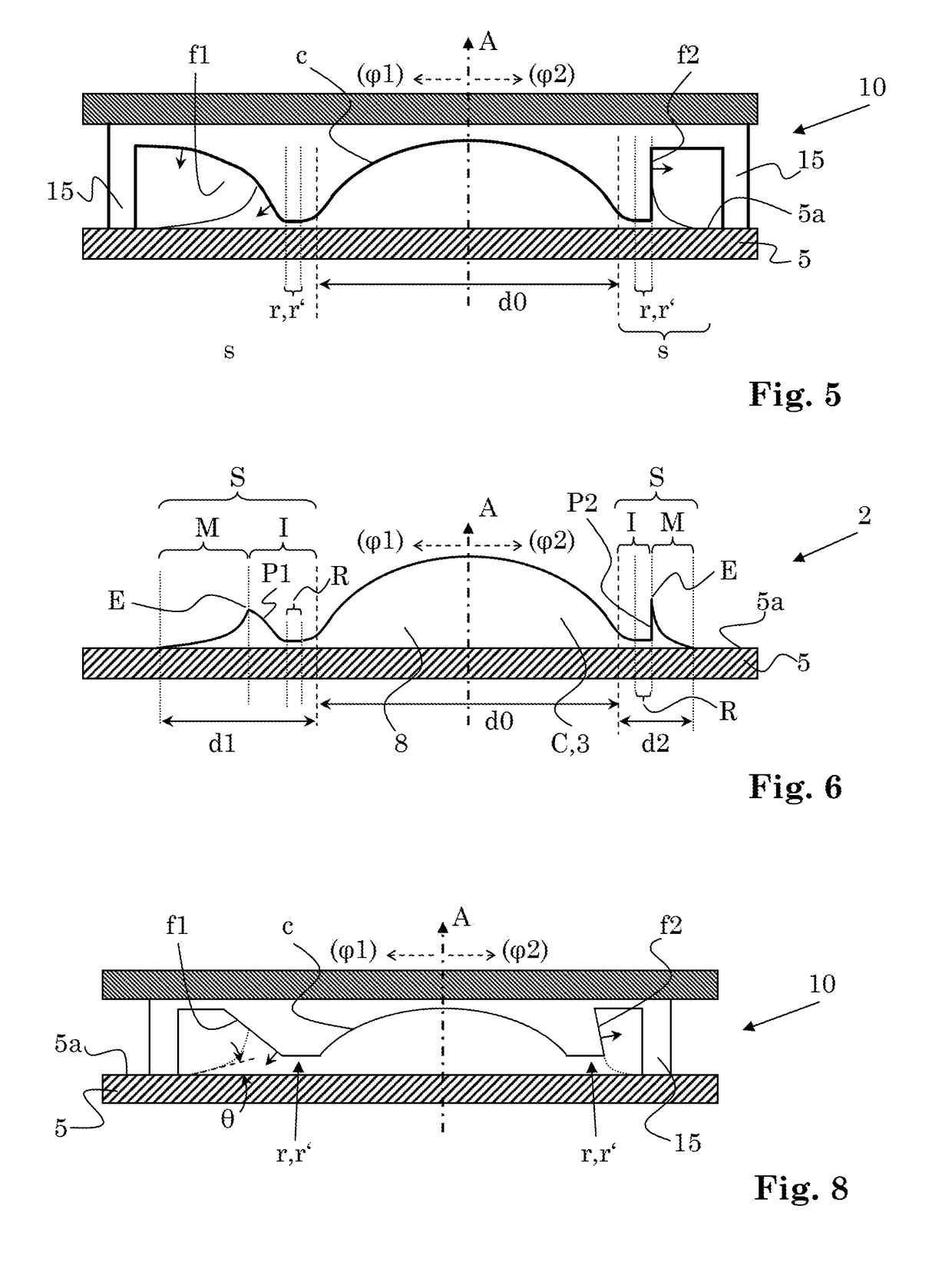
[0132]FIG. 1 is a schematized illustration of a cross-section through an optical device 1 which more particularly is an opto-electronic module. FIG. 2 is a schematized illustration of another cross-section through the optical device 1 of FIG. 1. In FIG. 2, the approximate position of the cross-section of FIG. 1 is indicated by the dashed line.

[0133]The optical device 1 includes a substrate 5 and another substrate 50 between which a spacer 20 is present which may be a part separate from the substrates 5 and 50, or may be constitute an integrally formed part, e.g., with substrate 50 as illustrated in FIG. 2.

[0134]On a first substrate surface 5a of substrate 5, two optical structures 2, 2′ are present which include an optical element 3 and 3′, respectively, each. In addition, another optical element is present on the other side of substrate 5.

[0135]On substrate 50, two active optical components 4, 4...


PUM

PropertyMeasurementUnit
contact angleaaaaaaaaaa

Abstract

A replication tool for producing an optical structure comprising an optical element includes a central section having the shape defining a negative of a portion of the optical structure and a vertically aligned central axis; a surrounding section laterally surrounding the central section; and one or more contact standoffs defining a plane referred to as contact plane. In a first azimuthal range, the surrounding portion provides a first compensation surface facing away from the central axis, and in a second azimuthal range, the surrounding portion provides a second compensation surface facing away from the central axis. In any cross-section containing the central axis in the second azimuthal range, a steepness of the second compensation surface is higher than a steepness of the first compensation surface in any cross-section containing the central axis in the first azimuthal range.

Description

BACKGROUND OF THE INVENTION[0001]Field of the Invention[0002]The invention relates to the field of optics, in of particular micro-optics, and more specifically to the manufacturing of optical components. More particularly, it relates to replication tools and to optical devices and to methods for manufacturing the same.[0003]Description of Related ArtDefinition of Terms[0004]“Active optical component”: A light sensing or a light emitting component. E.g., a photodiode, a photodiode array, an image sensor, an LED, an OLED, a laser chip. An active optical component can be present as a bare die or in a package, i.e. as a packaged component.[0005]“Passive optical component”: An optical component redirecting light by refraction and / or diffraction and / or (internal and / or external) reflection such as a lens, a prism, another diffractive or refractive structure, a mirror, or an optical system, wherein an optical system is a collection of such optical components possibly also including mechani...

Claims


Application Information

Patent Timeline
Patent Type & Authority Applications(United States)
IPC IPC(8): G02B3/00B29D11/00
CPCB29D11/00G02B3/0031B29D11/00307B29D11/0048
Inventor BIETSCH, ALEXANDERBARGE, MICHEL
Owner AMS SENSORS SINGAPORE PTE LTD
Why Eureka
Try Eureka