Check patentability & draft patents in minutes with Patsnap Eureka AI!

Memory device including a delay locked loop and operating method of the memory device

a memory device and locking loop technology, applied in the field of memory devices including locking loops and operating methods of memory devices, can solve the problems of time delay (or clock skew) and the inability to lock the time for synchronizing a clock phas

Active Publication Date: 2019-06-13
SAMSUNG ELECTRONICS CO LTD
View PDF1 Cites 2 Cited by
  • Summary
  • Abstract
  • Description
  • Claims
  • Application Information

AI Technical Summary

Benefits of technology

This patent describes a memory device with a delay locked loop (DLL) that can adjust the timing of a reference clock for normal and refresh modes of operation. The device also includes a data output circuit that uses the delayed reference clock to output data. The technical effects of this invention include improved data accuracy and reliability during normal and refresh modes, as well as efficient and effective memory device operation.

Problems solved by technology

When the externally applied clock is used in the memory device, a time delay (or a clock skew) may occur due to an internal circuit of the memory device.
However, when a voltage, a frequency, etc. associated with the internal circuits of the memory device varies, a locking time for synchronizing a clock phase may become long.

Method used


Image

  • Memory device including a delay locked loop and operating method of the memory device
  • Memory device including a delay locked loop and operating method of the memory device
  • Memory device including a delay locked loop and operating method of the memory device

Examples


Embodiment Construction

[0027]Exemplary embodiments of the inventive concept provide a memory device including a delay locked loop for quickly performing a locking operation and an operating method of the memory device.

[0028]Below, exemplary embodiments of the inventive concept will be described in detail with reference to the accompanying drawings. Like reference numerals may refer to like elements throughout this application.

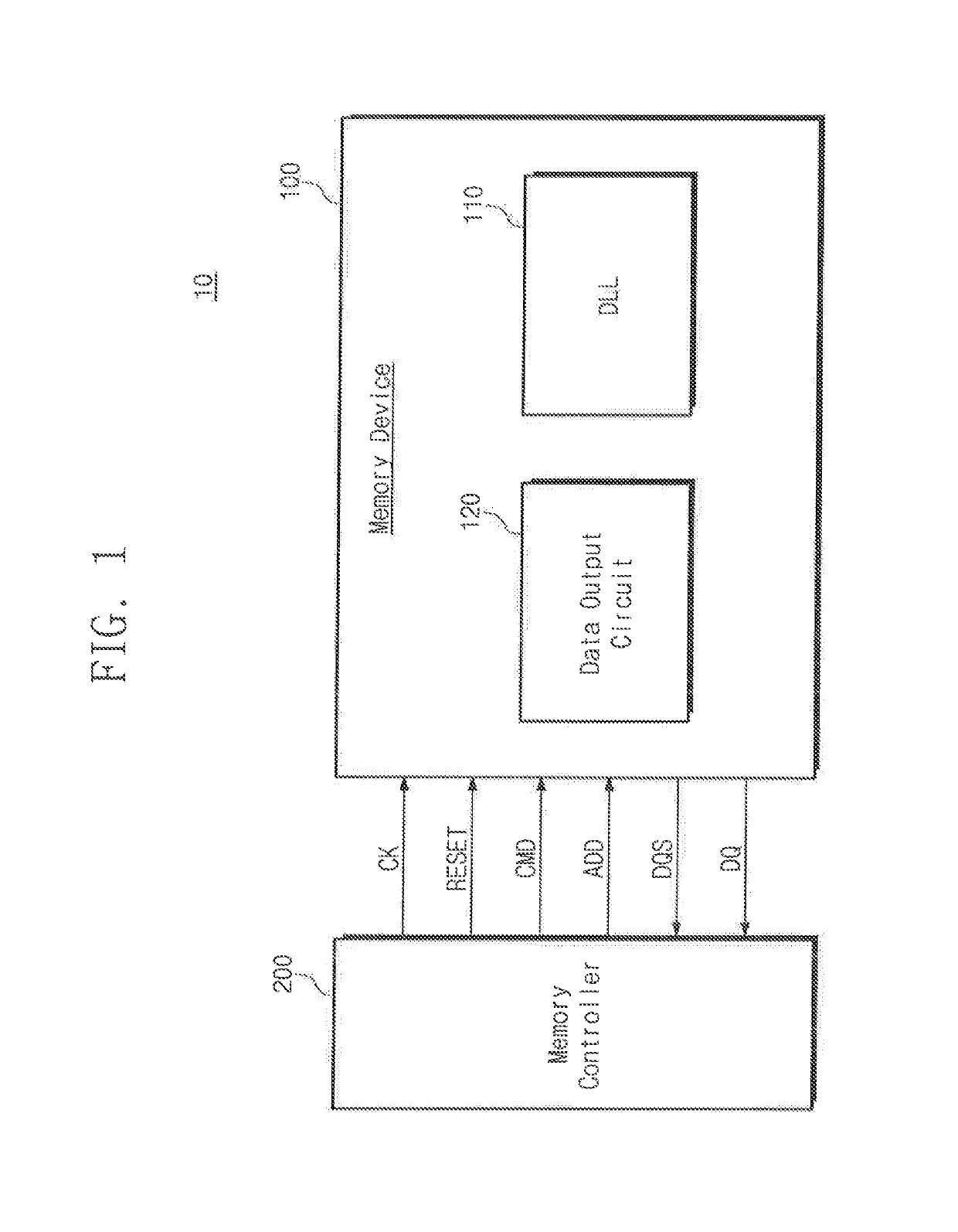
[0029]FIG. 1 is a block diagram of a semiconductor device according to an exemplary embodiment of the inventive concept. Referring to FIG. 1, a semiconductor device 10 may include a memory device 100 and a memory controller 200.

[0030]The memory device 100 may receive a clock signal CK, a reset signal RESET, a command CMD, and an address ADD from the memory controller 200. The memory device 100 may operate in synchronization with the clock signal CK. In an exemplary embodiment of the inventive concept, the memory device 100 may be a dynamic random access memory (DRAM). However, the in...


PUM


Abstract

A memory device includes a delay locked loop that generates a first code for delaying a reference clock in a first operation mode that is a normal operation mode, generates a second code for delaying the reference clock in a second operation mode that is a refresh mode, and delays the reference clock in response to one of the first and second codes depending on one of the first and second operation modes, and a data output circuit that outputs a data strobe signal (DQS) using the delayed reference clock.

Description

CROSS-REFERENCE TO RELATED APPLICATION[0001]This application claims priority under 35 U.S.C. § 119 to Korean Patent Application No. 10-2017-0168561, filed on Dec. 8, 2017 in the Korean Intellectual Property Office, the disclosure of which is incorporated by reference herein in its entirety.TECHNICAL FIELD[0002]Exemplary embodiments of the inventive concept described herein relate to a semiconductor memory device, and more particularly, relate to a memory device including a delay locked loop and an operating method of the memory device.DISCUSSION OF RELATED ART[0003]A semiconductor memory device may be classified as a volatile memory device or a nonvolatile memory device. A volatile memory device refers to a memory device that loses data stored therein at power-off. As an example of a volatile memory device, a dynamic random access memory (DRAM) may be used in various devices such as a mobile system, a server, or a graphic device.[0004]A memory device may operate in synchronization w...

Claims


Application Information

Patent Timeline
Patent Type & Authority Applications(United States)
IPC IPC(8): H03L7/081H03L7/08G11C7/22
CPCH03L7/0818H03L7/0805H03L7/0814G11C7/222G11C7/1066G11C11/406H03L7/0816G11C7/22
Inventor JUNG, HANGICHOI, HUN-DAEJEON, JUHO
Owner SAMSUNG ELECTRONICS CO LTD
Features
  • R&D
  • Intellectual Property
  • Life Sciences
  • Materials
  • Tech Scout
  • Unparalleled Data Quality
  • Higher Quality Content
  • 60% Fewer Hallucinations
Learn More