

Composition for semiconductor treatment and treatment method
Inactive Publication Date: 2019-06-27
JSR CORPORATIOON
View PDF12 Cites 3 Cited by
- Summary
- Abstract
- Description
- Claims
- Application Information
AI Technical Summary
Benefits of technology
The invention is a composition for treating semiconductors that can protect against corrosion and efficiently remove surface contamination. This composition is particularly useful when treating wiring boards that have tungsten wiring after chemical mechanical polishing. Overall, the patent provides a solution to prevent damage and improve the quality of semiconductor devices.
Problems solved by technology
When those polishing scraps remain on the object to be treated, a fatal device defect may occur.
Method used
View moreImage
Smart ImageViewing Examples

Examples
application example 2
[0014]In the treatment method according to the above-mentioned application example, the treatment method may further include diluting the composition for semiconductor treatment by from 20 times to 500 times.
application example 3
[0015]In the treatment method according to any one of the above-mentioned application examples, the treatment method may further include adjusting a viscosity of the composition for semiconductor treatment at 25° C. to 5 mPa·s or less.
application example 4
[0016]In the treatment method according to any one of the above-mentioned application examples, the treatment method may further include filtering the composition for semiconductor treatment with a depth-type filter or a pleat-type filter.
Login to View More PUM
 Abstract
Provided are a composition for semiconductor treatment capable of suppressing damage due to corrosion to wiring or the like including tungsten on an object to be treated, and efficiently removing contamination from a surface of the object to be treated, and a treatment method using the composition for semiconductor treatment. The treatment method includes a step of, after subjecting a wiring board including tungsten as a wiring material to chemical mechanical polishing using a composition containing an iron ion and a peroxide, subjecting the wiring board to treatment with a composition for semiconductor treatment which includes: a compound (A) having two or more of at least one selected from a group consisting of tertiary amino groups and salts thereof; and a water-soluble compound (B) having a solubility parameter of 10 or more, and which has a pH of from 2 to 7.
Description
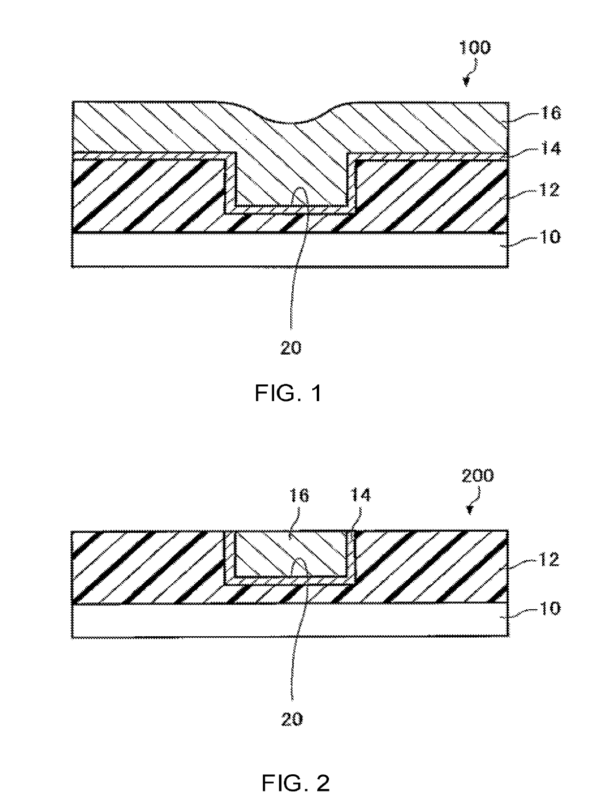
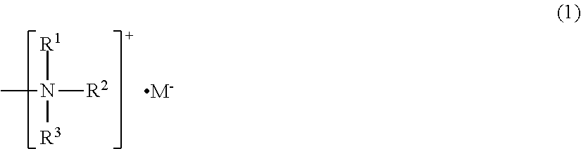
TECHNICAL FIELD[0001]The present invention relates to a composition for semiconductor treatment and a treatment method using the same.BACKGROUND ART[0002]Chemical mechanical polishing (CMP) utilized for production of semiconductor devices is a technology involving pressing an object to be treated (an object to be polished) against a polishing pad, and causing the object to be treated and the polishing pad to slide with respect to each other while supplying an aqueous dispersion for chemical mechanical polishing (hereinafter also referred to simply as “CPM slurry”) onto the polishing pad, to thereby chemically and mechanically polish the object to be treated. The CMP slurry used for such CMP contains a chemical, such as an etching agent or a pH adjusting agent, as well as abrasive grains for polishing. Moreover, polishing scraps are generated through the CMP. When those polishing scraps remain on the object to be treated, a fatal device defect may occur. Therefore, a step of cleaning...
Claims
Login to View More Application Information
Patent Timeline
 IPC IPC(8): C09G1/04H01L21/321H01L21/02H01L21/768
CPCC09G1/04H01L21/3212H01L21/02074H01L21/7684H01L21/76883B24B37/00
InventorYOKOI, KATSUTAKAYAMAMOTO, KEN-ICHIMITSUBOSHI, RANMASUDA, KANAEKAMO, SATOSHISHINODA, TOMOTAKA
OwnerJSR CORPORATIOON