
Display panel

a technology of display panel and substrate, which is applied in the field of display panel, can solve the problems of less display area for a particular, conductive routing lines or paths that are usually required for the substrate of a conventional display panel, and achieve the effect of reducing the required peripheral area and being larger viewabl

Inactive Publication Date: 2019-06-27
NOVATEK MICROELECTRONICS CORP
View PDF11 Cites 1 Cited by
  • Summary
  • Abstract
  • Description
  • Claims
  • Application Information

AI Technical Summary

Benefits of technology

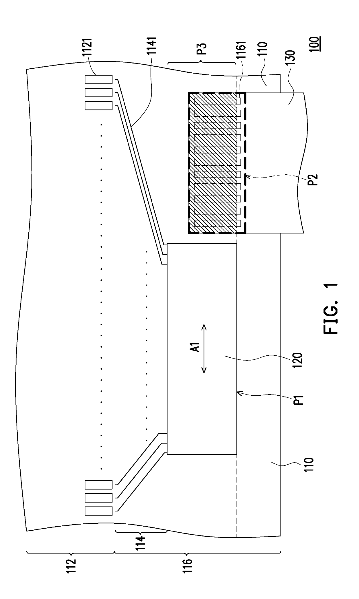
The invention describes a design for a display panel with a smaller peripheral area, which allows for a narrower bezel and a larger viewable display area. This is achieved by placing the chip region and the connecting region for bonding the FPC board in the peripheral area, which is then extended along the longitudinal axis of the chip through an extensional region. The connecting region overlaps with the extensional region, reducing the required space for the peripheral area and resulting in a narrower bezel. Overall, this design provides a larger viewable display area for the display panel.

Problems solved by technology

However, one problem is that a substrate of a conventional display panel usually requires relatively wide conductive routing lines or paths (e.g., 3-5 microns wide).
With a design rule for the driver IC and routing paths of the routing lines, the bezel size can be undesirably large, resulting in less room for the display area for a particular size of display backplane.

Method used


Image

  • Display panel
  • Display panel
  • Display panel

Examples


Embodiment Construction

[0026]Reference will now be made in detail to the present preferred embodiments of the disclosure, examples of which are illustrated in the accompanying drawings. Wherever possible, the same reference numbers are used in the drawings and the description to refer to the same or like parts. The terms used herein such as “on”, “above”, “below”, “front”, “back”, “left” and “right” are for the purpose of describing directions in the figures only and are not intended to be limiting of the disclosure.

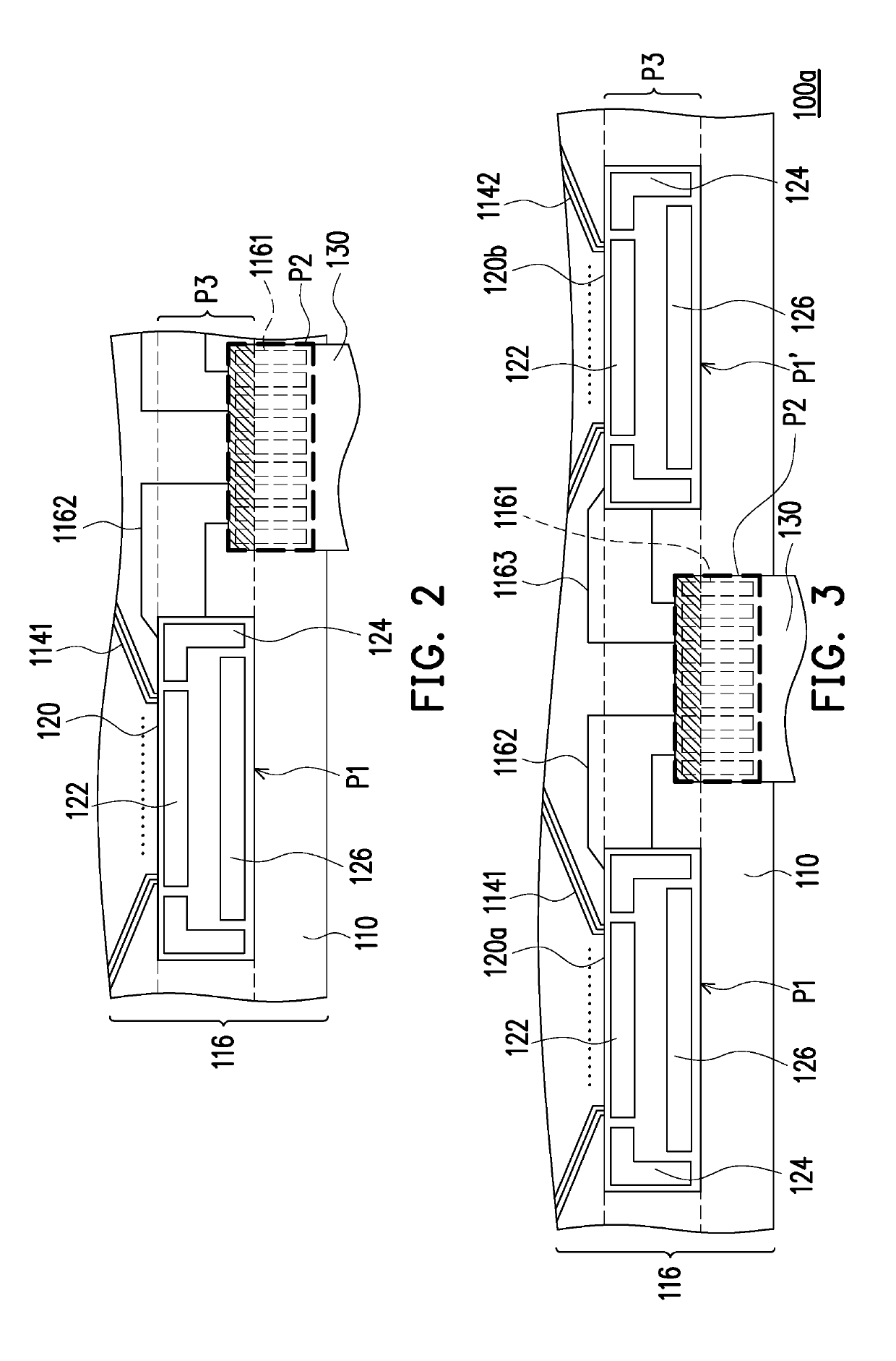
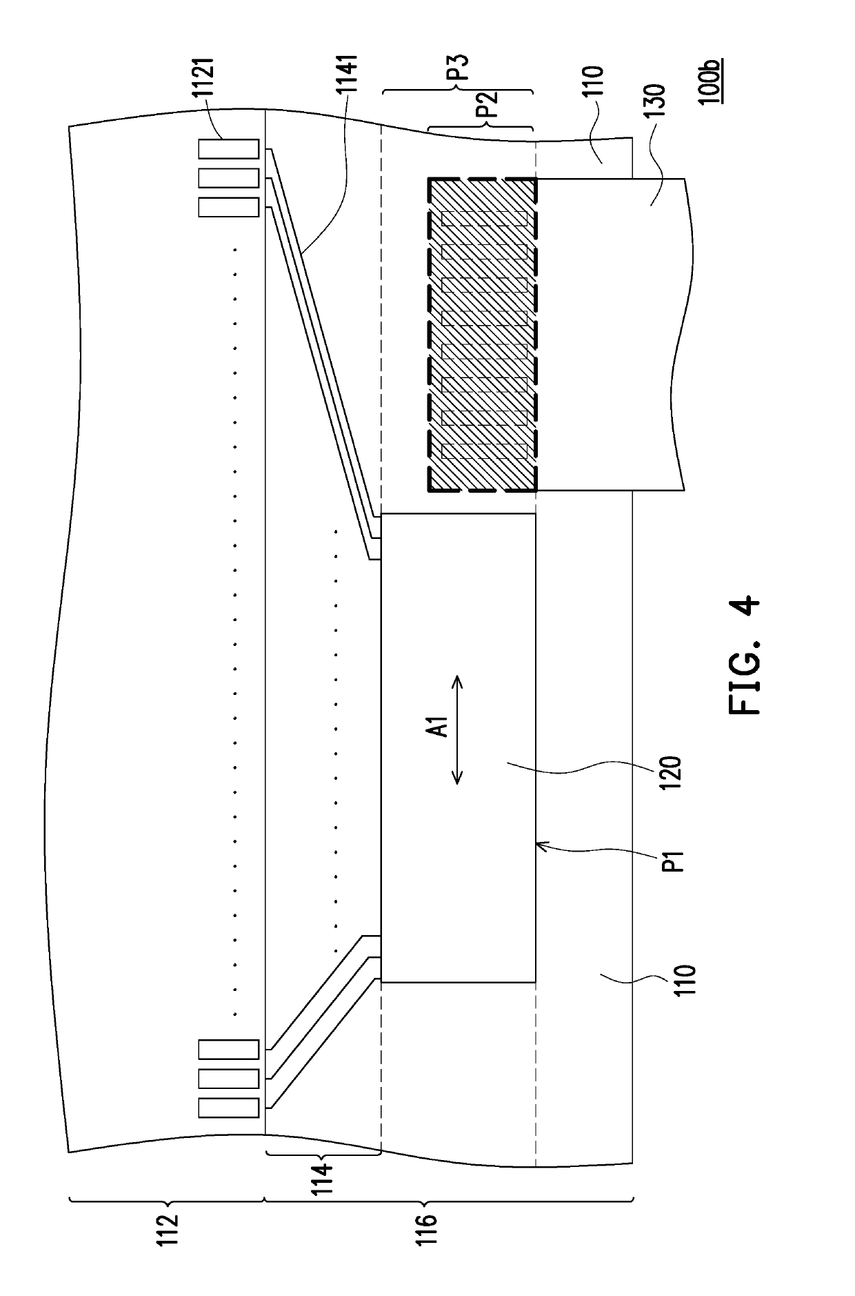
[0027]FIG. 1 illustrates a schematic view of a display panel according to an embodiment of the disclosure. FIG. 2 illustrates a partial enlarged of a display panel according to an embodiment of the disclosure. Referring to FIG. 1 and FIG. 2, in the present embodiments, the display panel 100 may be a liquid crystal display (LCD) panel, an organic light emitting diode (OLED) display panel, or any other display panels applicable. The display panel 100 includes a substrate 110, at least one chip 1...


PUM


Abstract

A display panel includes a substrate, a chip, a connecting portion, and a plurality of connecting lines. The substrate includes an active area where a pixel array is located and a peripheral area at a side of the active area. The peripheral area includes a chip region and a connecting region. The chip is mounted on the chip region of the peripheral area and electrically connected to the pixel array. The connecting portion is disposed on the connecting region of the peripheral area and configured to electrically connect a flexible printed circuit (FPC) board. The connecting region is overlapped with an extensional region extended from the chip region along a longitudinal axis of the chip. The connecting lines are electrically connecting the chip and the connecting portion.

Description

CROSS-REFERENCE TO RELATED APPLICATION[0001]This application claims the priority benefit of U.S. provisional application Ser. No. 62 / 610,292, filed on Dec. 26, 2017. The entirety of the above-mentioned patent application is hereby incorporated by reference herein and made a part of this specification.BACKGROUNDTechnical Field[0002]The present disclosure generally relates to a display panel. More particularly, the present disclosure relates to a display panel with narrow bezel.Description of Related Art[0003]A display typically includes of an array (or matrix) of picture elements (“pixels”). Thousands or millions of these pixels together create an image on the display. The light modulators of the pixels are electronically driven by drive components, e.g., driver IC chips, which are located on the periphery of a display panel. A drive IC chip uses contact pads to connect with routing lines that conduct electrical signals to drive each row and column of the array of picture elements.[0...

Claims


Application Information

Patent Timeline
Patent Type & Authority Applications(United States)
IPC IPC(8): G09G3/20H05K1/18
CPCG09G3/20H05K1/189H05K2201/10128G09G2300/0426G09G2300/0408G09G3/3208G09G3/36H05K1/147
Inventor KUO, I-CHUNTZENG, SYANG-YUN
Owner NOVATEK MICROELECTRONICS CORP
Learn More