Supercharge Your Innovation With Domain-Expert AI Agents!

Light emitting device

a light-emitting device and light-emitting technology, applied in the field of optical technologies, can solve problems such as reducing the luminous efficiency of light-emitting devices

Active Publication Date: 2019-06-27
NANJING TECH CORP LTD
View PDF4 Cites 6 Cited by
  • Summary
  • Abstract
  • Description
  • Claims
  • Application Information

AI Technical Summary

Benefits of technology

The present patent describes a light emitting device that includes a pixel isolation structure and electroluminescent structures. The device also includes a quantum dot layer in each sub-pixel region, which is isolated from adjacent layers through the pixel isolation structure. This prevents any unwanted light from being emitted and increases the luminous efficiency of the device. The technical effect of this invention is improved efficiency and accuracy in the production of light emitting devices.

Problems solved by technology

However, the black matrix has a disadvantage of absorbing light, thereby reducing the luminous efficiency of the light emitting device.

Method used


Image

  • Light emitting device
  • Light emitting device
  • Light emitting device

Examples


embodiments

Embodiment 1

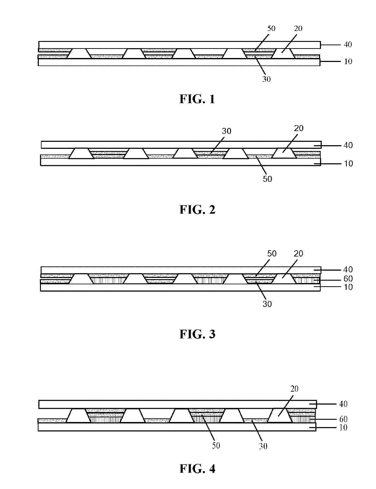
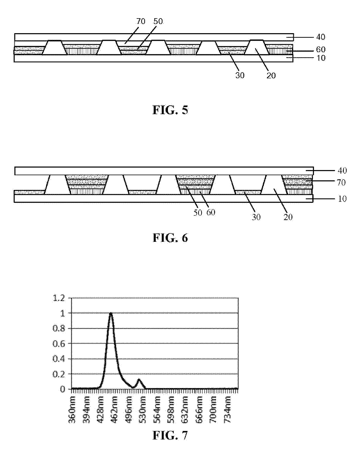
[0049]The light emitting device provided in this embodiment is a top emitting device, including a first substrate, a pixel isolation structure, an electroluminescent structure, a quantum dot layer and a second substrate, wherein the second substrate is disposed opposite to the first substrate, and the pixel isolation structure is disposed on the surface of one side of the first substrate, and the second substrate is disposed on one side of the pixel isolation structure far away from the first substrate; the pixel isolation structure isolates pixels on the first substrate to form six sub-pixel regions including three types of sub-pixel region, namely, R, G, and B, wherein the part of the first substrate corresponding to the B (blue) sub-pixel region is only disposed with the electroluminescent structure, and the R (red) sub-pixel region and the G (green) sub-pixel region adjacent to the B sub-pixel region are further disposed with the quantum dot layer; the electrolumines...

embodiment 2

[0051]The difference of the light emitting device provided in this embodiment and Embodiment 1 is as follows:

[0052]The width of the quantum dot layer in each sub-pixel region is greater than the width of the effective light emitting region of the electroluminescent structure.

embodiment 3

[0053]The difference of the light emitting device provided in this embodiment and Embodiment 2 is as follows:

[0054]The light emitting device further includes first padding portion, wherein the quantum dot layer in each sub-pixel region is located on one side of the electroluminescent structure far away from the first substrate, and the first padding portion and the quantum dot layer are disposed in different sub-pixel regions respectively and located between the first substrate and the electroluminescent structure, a first distance defined as the shortest distance between the surface of the quantum dot layer and the surface of the first substrate, a second distance defined as the shortest distance between the surface of the light emitting layer located in the same sub-pixel region as the first padding portion and the surface of the first substrate, the first distance is equal to the second distance, wherein the first padding portion is a SiO2 layer.


PUM


Abstract

Embodiments disclosed herein relate to a light emitting device, comprising a first substrate, a pixel isolation structure, electroluminescent structures, and a second substrate, the first substrate and the second substrate are oppositely disposed, and the second substrate is disposed on one side of pixel isolation structure far away from the first substrate, the pixel isolation structure is disposed on the surface of one side of first substrate, the pixel isolation structure forms a plurality of mutually isolated sub-pixel regions on the surface of first substrate, electroluminescent structures are disposed on a portion of first substrate corresponding to each sub-pixel region, the sub-pixel regions further comprise: a quantum dot layer disposed in at least one sub-pixel region, wherein quantum dot layer in each sub-pixel region is located on one side of electroluminescent structures far away from first substrate or located between electroluminescent structure and first substrate.

Description

CROSS REFERENCE TO RELATED APPLICATIONS[0001]This application is a national application of PCT / CN2017099524, filed on Aug. 29, 2017. The contents of PCT / CN2017099524 are all hereby incorporated by reference.TECHNICAL FIELD[0002]The present disclosure relates to the field of optical technologies, and in particular to a light emitting device.BACKGROUND[0003]The application of quantum dots in display devices mainly includes quantum dot photoluminescent backlight system and quantum dot electroluminescent structure (QLED). At present, since the quantum dot efficiency of the quantum dot electroluminescent structure still does not meet the market demand, people have begun to explore a light emitting device combining photoluminescence and electroluminescence, wherein an electroluminescent sub-pixel corresponds to a photoluminescent quantum dot layer, and a light with a first wavelength generated after the electroluminescent sub-pixel is energized passes through the photoluminescent quantum ...

Claims


Application Information

Patent Timeline
Patent Type & Authority Applications(United States)
IPC IPC(8): H01L51/50H01L51/52
CPCH01L51/502H01L51/52H01L2251/5315H01L2251/533H10K50/115H10K59/80H10K59/8723H10K59/38H10K59/122H10K2102/331H10K2102/351H10K59/871H10K50/00H10K50/80H10K2102/3026H10K2102/3035
Inventor DU, YONG
Owner NANJING TECH CORP LTD
Features
  • R&D
  • Intellectual Property
  • Life Sciences
  • Materials
  • Tech Scout
  • Unparalleled Data Quality
  • Higher Quality Content
  • 60% Fewer Hallucinations
Learn More