Optical guide comprising a bend with a pseudo-index gradient

Active Publication Date: 2019-07-11
COMMISSARIAT A LENERGIE ATOMIQUE ET AUX ENERGIES ALTERNATIVES
View PDF0 Cites 2 Cited by
  • Summary
  • Abstract
  • Description
  • Claims
  • Application Information

AI Technical Summary

Benefits of technology

The invention aims to use wide guides to direct light in a photonic circuit, reducing losses and minimizing the size of the circuit. This will make it possible to create more efficient and compact devices.

Problems solved by technology

This gain in terms of losses, however, poses a problem for the guiding.
Indeed, only the narrow guides allow management, with reasonable losses, of the curves.

Method used


Image

  • Optical guide comprising a bend with a pseudo-index gradient
  • Optical guide comprising a bend with a pseudo-index gradient
  • Optical guide comprising a bend with a pseudo-index gradient

Examples


Embodiment Construction

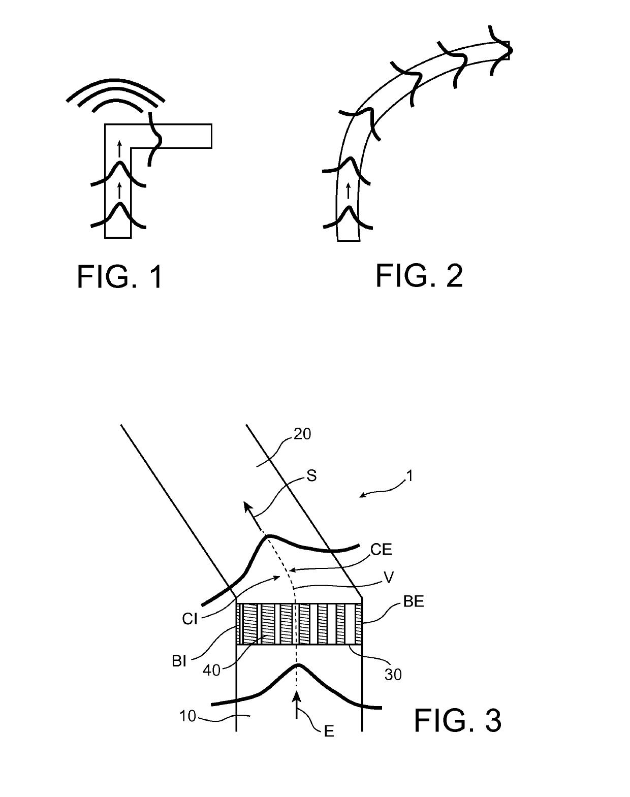
[0025]FIG. 1 shows a diagram of an optical guide integrating a break between two rectilinear optical paths, in the form of an abrupt bend of 90°. With such a right-angle break, the light is confronted with strong radiation losses, whether the guide is narrow or wide. In order to prevent such a break, it is thus possible to resort to a curve having a large radius as is shown in FIG. 2. The transfer of the electromagnetic field out of the guide is thus minimised, but to the detriment of the compactness.

[0026]FIG. 3 shows a diagram of an optical guide 1 according to the invention in which the light is deviated while preserving a uniform wave front.

[0027]According to the invention, the optical guide 1 can be a planar waveguide (“Planar waveguide” or “Slab waveguide” in the Anglo-Saxon terminology), a channel waveguide (“Ridge waveguide” in the Anglo-Saxon terminology), or a rib waveguide (“Rib waveguide” in the Anglo-Saxon terminology).

[0028]The optical guide 1 comprises a core made fro...


PUM


Abstract

An optical guide comprising a core that has a entrance segment that is rectilinear in an entrance direction, an exit segment that is rectilinear in an exit direction, and a transition segment between the rectilinear entrance segment and the rectilinear exit segment. The exit direction is different from the entrance direction so that light propagates between the entrance segment and the exit segment in a propagation direction that has a bend having an interior side and an exterior side. The transition segment comprises a region with a pseudo-index gradient, this region having an interior edge on the interior side of the bend and an exterior edge on the exterior side of the bend. The region with the pseudo-index gradient comprises trenches formed in the core in order to make a refractive index decrease from the interior edge to the exterior edge.

Description

TECHNICAL FIELD[0001]The field of the invention is that of structures for guiding light used in photonic and optoelectronic circuits. The invention relates more particularly to guiding structures in which the light is subjected to a change in direction by the introduction of a break or of a curved trajectory between two rectilinear paths.PRIOR ART[0002]The propagation of optical signals on a chip requires a good compromise between losses and compactness. According to the intended use, the total optical path can vary between several millimetres for a single function (emission, modulation, filtering, photo-detection) and a plurality of centimetres for the most complex circuits.[0003]In this context, silicon photonics provide, in addition to the compatibility with electronics, a platform that is extremely efficient via the strong refractive index contrast of the waveguides between the core (generally made of silicon) and the cladding (generally made of silica) which results in very low...

Claims


Application Information

Patent Timeline
IPC IPC(8): G02B6/125
CPCG02B6/125G02B2006/12119G02B6/14
Inventor HASSAN, KARIMBOUTAMI, SALIM
Owner COMMISSARIAT A LENERGIE ATOMIQUE ET AUX ENERGIES ALTERNATIVES
Why Eureka
Try Eureka