Method of forming integrated circuit with gate-all-around field effect transistor and the resulting structure

a field effect transistor and integrated circuit technology, applied in the field of integrated circuits (ic), can solve the problems of no longer allowing for proper formation of epitaxial source/drain region, no longer suitable processing techniques for aafets, etc., and achieve the effect of reducing siz

Active Publication Date: 2019-07-11
GLOBALFOUNDRIES US INC
View PDF12 Cites 24 Cited by
  • Summary
  • Abstract
  • Description
  • Claims
  • Application Information

AI Technical Summary

Benefits of technology

[0003]In view of the foregoing, disclosed herein are method embodiments for forming an integrated circuit (IC) structure having at least one gate-all-around field effect transistor (GAAFET) and, particularly, at least one nanowire-type field effect transistor (NWFET). In the method embodiments, a sacrificial gate can be formed on a multi-layer fin. Then, sidewall spacer processing can be performed such that a gate section of a sidewall spacer is formed on the sacrificial gate and fin sections are formed on exposed portions of the fin. Either before or after selective removal of the exposed portions of the fin, the fins sections of the sidewall spacer can be completely removed or at least reduced in size without significantly impacting the integrity of the gate section. As a result, the areas within which the transistor source / drain regions are to be formed will not be bound by the original fin sections of the sidewall spacer. Furthermore, any isolation material, which is deposited into these areas prior to epitaxial source / drain region formation and which is used to form the isolation elements that will provide electrical isolation between the transistor gate and source / drain regions, can be selectively removed without impacting the integrity of the isolation elements. Thus, the method embodiments include processes that allow for device size scaling while still ensuring proper formation of epitaxial source / drain regions. Techniques are also disclosed for the simultaneous formation, on the same semiconductor substrate, of different types of GAAFET (e.g., one or more nanosheet-type field effect transistors (NSFETs)) and / or fin-type field effect transistor (FINFETs). Also disclosed herein are IC structure embodiments formed using the above-described method.

Problems solved by technology

However, with continued device size scaling, conventional GAAFET processing techniques may no longer be suitable and, particularly, may no longer allow for proper formation of epitaxial source / drain regions.

Method used


Image

  • Method of forming integrated circuit with gate-all-around field effect transistor and the resulting structure
  • Method of forming integrated circuit with gate-all-around field effect transistor and the resulting structure
  • Method of forming integrated circuit with gate-all-around field effect transistor and the resulting structure

Examples


Embodiment Construction

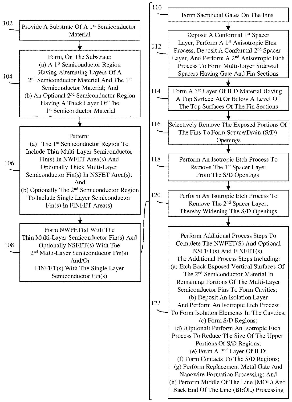
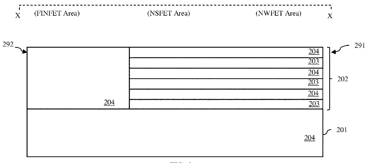
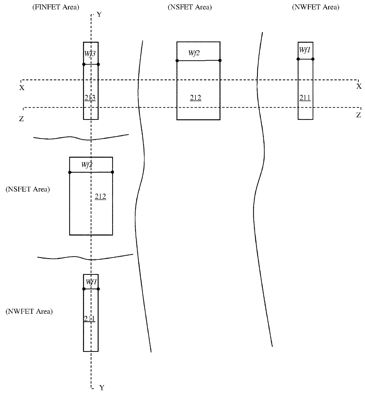
[0038]As mentioned above, integrated circuit (IC) design decisions are often driven by device performance, scalability, and manufacturability. For example, recently, to improve device drive current and electrostatics and to allow for further device size scaling, gate-all-around field effect transistors (GAAFETs) (e.g., nanowire-type GAAFETs or nanosheet-type GAAFETs) were developed. A GAAFET includes elongated nanoshape(s) (e.g., nanowires or nanosheets), which extend laterally between source / drain regions, and a gate structure, which wraps around the nanoshape(s) (i.e., which is adjacent to the top, bottom and two opposing sides of the each nanoshape) such that the nanoshape(s) function as channel region(s). However, with continued device size scaling, conventional GAAFET processing techniques may no longer be suitable and, particularly, may no longer allow for proper formation of epitaxial source / drain regions.

[0039]Specifically, current GAAFET processing techniques begin with a s...


PUM


Abstract

Disclosed are methods for forming an integrated circuit with a nanowire-type field effect transistor and the resulting structure. A sacrificial gate is formed on a multi-layer fin. A sidewall spacer is formed with a gate section on the sacrificial gate and fin sections on exposed portions of the fin. Before or after removal of the exposed portions of the fin, the fins sections of the sidewall spacer are removed or reduced in size without exposing the sacrificial gate. Thus, the areas within which epitaxial source/drain regions are to be formed will not be bound by sidewall spacers. Furthermore, isolation material, which is deposited into these areas prior to epitaxial source/drain region formation and which is used to form isolation elements between the transistor gate and source/drain regions, can be removed without removing the isolation elements. Techniques are also disclosed for simultaneous formation of a nanosheet-type and/or fin-type field effect transistors.

Description

BACKGROUNDField of the Invention[0001]The present invention relates to integrated circuits (IC) and, more particularly, to embodiments of a method for forming an IC that includes at least one gate-all-around field effect transistor (GAAFET) and to embodiments of an IC structure formed according to the method.Description of Related Art[0002]Integrated circuit (IC) design decisions are often driven by device performance, scalability, and manufacturability. For example, recently, to improve device drive current and electrostatics and to allow for further device size scaling, gate-all-around field effect transistors (GAAFETs) (e.g., nanowire-type GAAFETs or nanosheet-type GAAFETs) were developed. A GAAFET includes elongated nanoshape(s) (e.g., nanowires or nanosheets), which extend laterally between source / drain regions, and a gate structure, which wraps around the nanoshape(s) (i.e., which is adjacent to the top, bottom and two opposing sides of the each nanoshape) such that the nanosh...

Claims


Application Information

Patent Timeline
Patent Type & Authority Applications(United States)
IPC IPC(8): H01L29/423H01L29/66H01L21/306H01L21/762H01L21/311H01L21/3105H01L21/768H01L21/8234H01L29/06H01L29/78H01L29/10H01L29/08H01L27/088H01L27/02
CPCH01L29/42392H01L29/66795H01L29/66545H01L29/66636H01L29/6656H01L21/30604H01L21/76224H01L21/31111H01L21/31053H01L21/76897H01L21/823431H01L29/0673H01L29/7851H01L29/1033H01L29/0847H01L29/0649H01L21/823418H01L21/823437H01L21/823481H01L21/823412H01L27/0886H01L27/0207H01L29/775H01L29/41791H01L29/785H01L29/78696H01L29/66439B82Y10/00H01L29/0653H01L29/41725
Inventor XIE, RUILONGPRANATHARTHIHARAN, BALASUBRAMANIANMONTANINI, PIETROFROUGIER, JULIEN
Owner GLOBALFOUNDRIES US INC
Why Eureka
Try Eureka