Switching device, method of fabricating the same, and non-volatile memory device having the same

a switching device and non-volatile memory technology, applied in the field of switching devices, can solve the problems of cross talk associated with memory write errors and read errors, and achieve the effects of stable non-linear resistance paths, low operating voltage, and high on/off current ratio

Active Publication Date: 2019-07-18
SK HYNIX INC +1
View PDF4 Cites 3 Cited by
  • Summary
  • Abstract
  • Description
  • Claims
  • Application Information

AI Technical Summary

Benefits of technology

[0021]According to an embodiment of the present invention, a switching film including an electrically insulating matrix and a conductive path formed in the electrically insulating matrix is embedded. The conductive path is provided by the crystalline metal clusters that are dispersed within the electrically insulating matrix, and a metal bridge connecting adjacent metal clusters. Therefore, a stable non-linear resistance path can be provided in the electrically insulating matrix, and as a result, a switching device having a low operating voltage, high on/off current ratio (Ion/off), a high...

Problems solved by technology

However, there is a possibility that cross talk associated with memory write errors...

Method used


Image

  • Switching device, method of fabricating the same, and non-volatile memory device having the same
  • Switching device, method of fabricating the same, and non-volatile memory device having the same
  • Switching device, method of fabricating the same, and non-volatile memory device having the same

Examples


Embodiment Construction

[0033]Hereinafter, preferred embodiments of the present invention will be described in detail with reference to the accompanying drawings.

[0034]Embodiments of the present invention are provided to the person skilled in the art in order to explain the present invention more completely well. The following embodiments may be modified in various other forms, and the scope of the present invention is not limited to the following embodiments. Rather, these embodiments are provided so that this disclosure may be described more faithfully and completely, and may fully convey the concept of the invention to those skilled in the art.

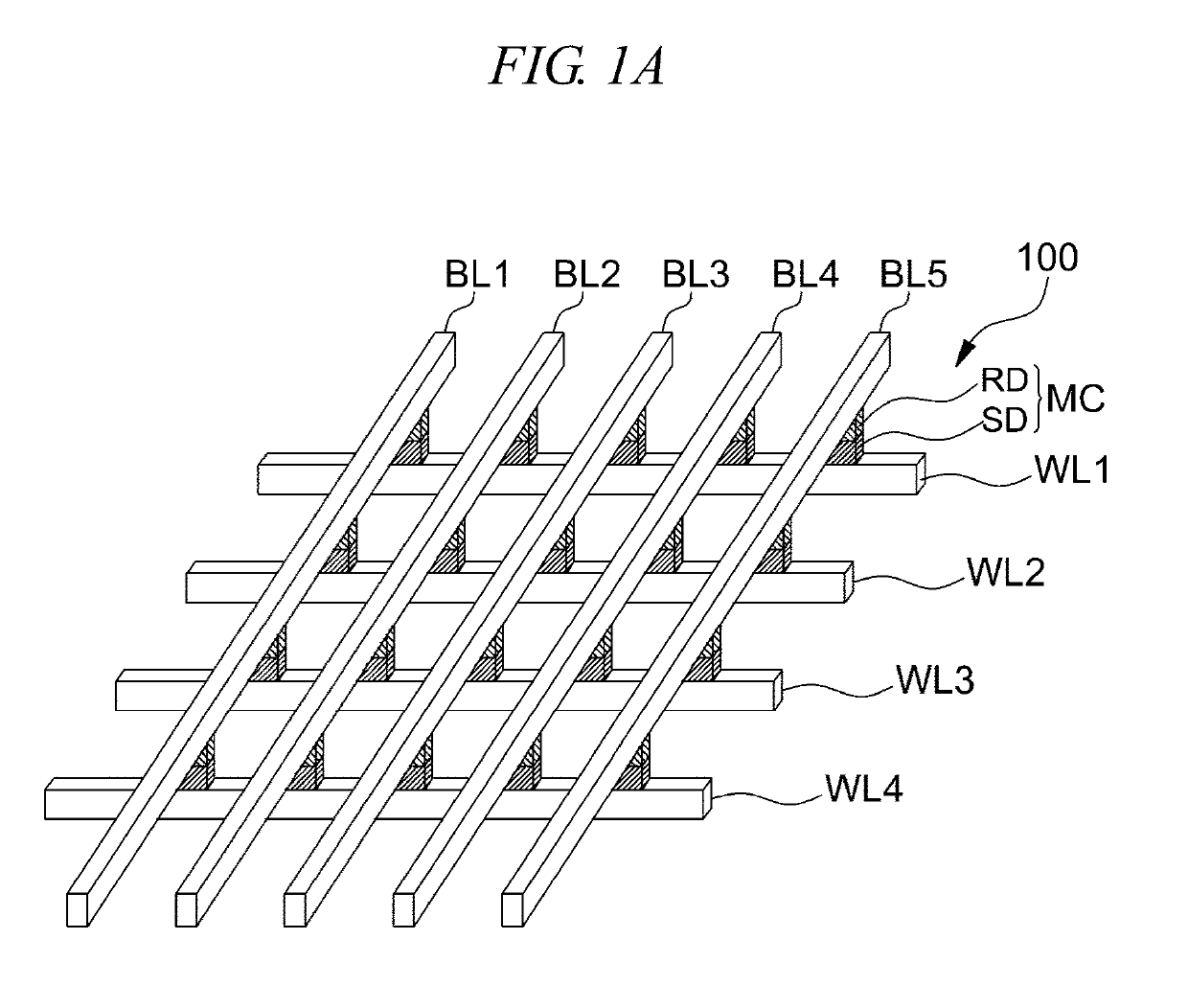
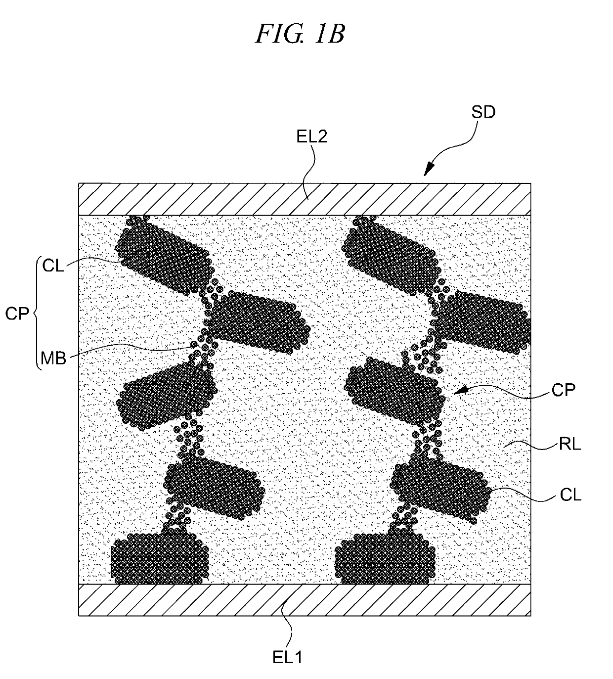
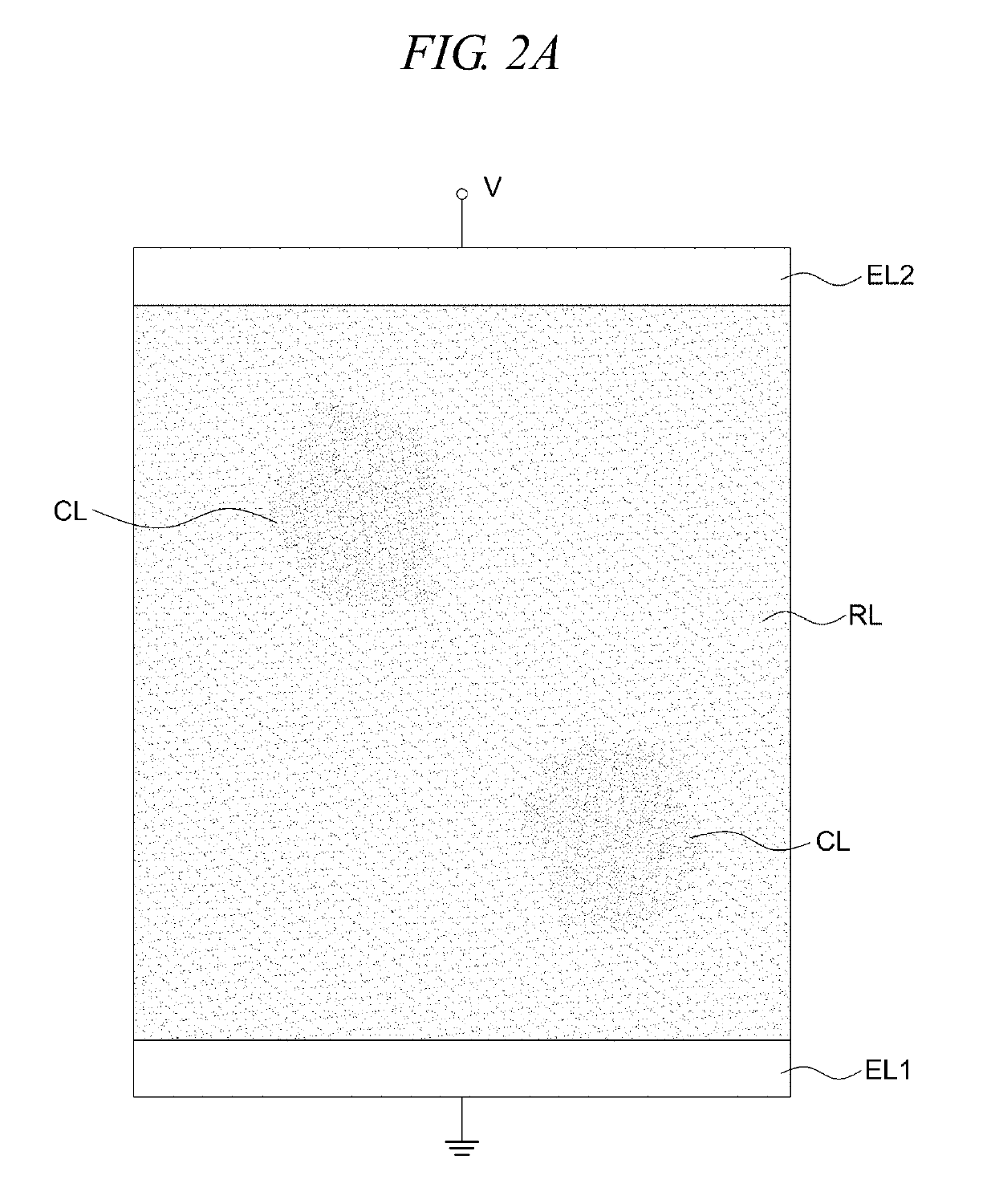
[0035]Further, in the following drawings, the thickness and the size of each layer are exaggerated for convenience of description and clarity of explanation. The same reference numerals refer to the same elements in the drawings. As used herein, the term “and / or” includes any one of the listed items and all combinations of more than one item.

[0036]The terms used h...


PUM


Abstract

The present invention relates to a switching device, a method of fabricating the same, and a nonvolatile memory device including the same. A switching device according to an embodiment of the present invention includes a first electrode; a second electrode; and a switching film which is disposed between the first electrode and the second electrode, and includes an electrically insulating matrix and a conductive path formed in the electrically insulating matrix. In this embodiment, the conductive path includes crystalline metal clusters dispersed in the electrically insulating matrix and a metal bridge connecting adjacent crystalline metal clusters.

Description

CROSS-REFERENCES TO RELATED APPLICATION[0001]The present application claims priority under 35 U.S.C. 119(a) to the Korean application number 10-2018-0006417 filed on Jan. 18, 2018, which is herein incorporated by reference in its entirety.BACKGROUND OF THE INVENTIONField[0002]The present invention relates to semiconductor technology, and more particularly, a switching device, a method of fabricating the same, and a nonvolatile memory device having the same.2. Description of the Related Art[0003]In recent years, the nonvolatile memory market is rapidly expanding as demand for portable digital applications such as digital cameras, MP3 players, and smart phones increases. As a programmable non-volatile memory device, a NAND flash memory is a typical example, and techniques such as a three-dimensional memory structure and a multi-level cell (MLC) are being actively developed to improve integration density. However, as NAND flash memory reaches the limit of scaling, as a new nonvolatile ...

Claims


Application Information

Patent Timeline
IPC IPC(8): H01L45/00H01L27/24H01L27/22
CPCH01L45/10H01L45/1641H01L27/2409H01L27/224H01L45/14H01L45/1233H10B61/10H10B63/20H10N70/245H10N70/881H10N70/826H10N70/023H10N70/026H10N70/041H01L29/788H10N70/841H10N70/883H10N70/011H10N70/25
Inventor KIM, HYEONG JOONPARK, JI WOONKIM, YOUNG SEOK
Owner SK HYNIX INC
Why Eureka
Try Eureka