

Field effect transistor and method for manufacturing the same
- Summary
- Abstract
- Description
- Claims
- Application Information
AI Technical Summary
Benefits of technology
Problems solved by technology
Method used
Image

Examples
Embodiment Construction
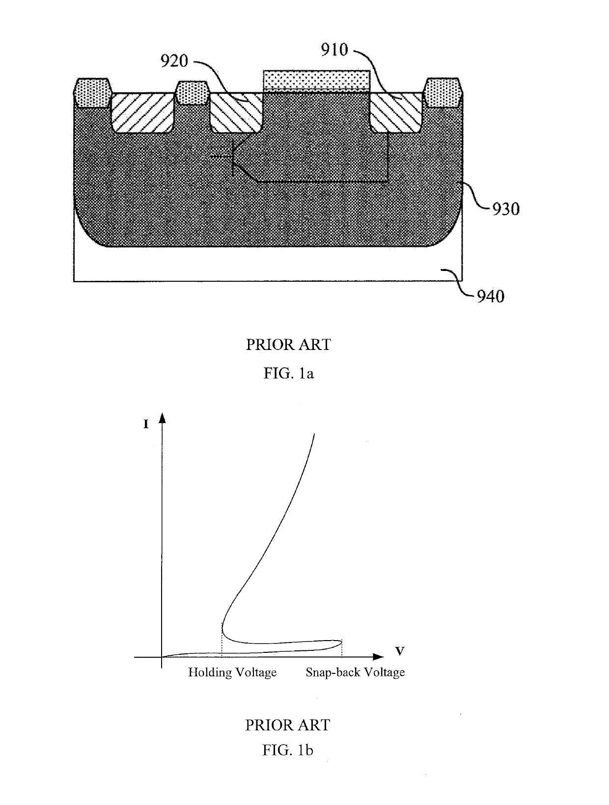
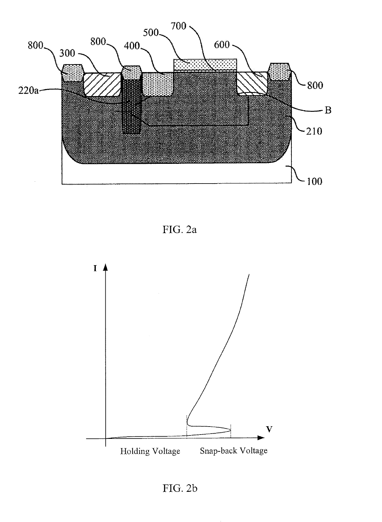
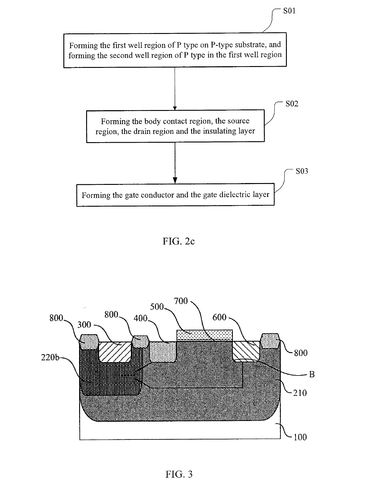
[0041]Exemplary embodiments of the present disclosure will be described in more details below with reference to the accompanying drawings. In the drawings, like reference numerals denote like members. The figures are not drawn to scale, for the sake of clarity. Moreover, some well-known parts may not be shown. For simplicity, the structure of the semiconductor device having been subject to several relevant process steps may be shown in one figure.
[0042]It should be understood that when one layer or region is referred to as being “above” or “on” another layer or region in the description of device structure, it can be directly above or on the other layer or region, or other layers or regions may be intervened therebetween. Moreover, if the device in the figures is turned over, the layer or region will be under or below the other layer or region.
[0043]In contrast, when one layer is referred to as being “directly on” or “on and adjacent to” or “adjoin” another layer or region, there ar...
PUM
 Abstract
Description
Claims
Application Information