METAL SILICIDE SELF-ALIGNED SiGe HETEROJUNCTION BIPOLAR TRANSISTOR AND METHOD OF FORMING THE SAME

Inactive Publication Date: 2013-11-28
TSINGHUA UNIV
View PDF2 Cites 6 Cited by
  • Summary
  • Abstract
  • Description
  • Claims
  • Application Information

AI Technical Summary

Benefits of technology

[0010]To overcome the aforesaid shortcomings, the present invention provides a metal silicide self-aligned

Problems solved by technology

However, because silicon materials are inherently disadvantageous in speed, group III-V compound (e.g., gallium arsenide) semiconductor devices have always dominated in the field of high-frequency and high-speed applications in the history.
The former technical solution requires use of expensive special planarization apparatuses and processes; and the latter technical solution may cause proces

Method used


Image

  • METAL SILICIDE SELF-ALIGNED SiGe HETEROJUNCTION BIPOLAR TRANSISTOR AND METHOD OF FORMING THE SAME
  • METAL SILICIDE SELF-ALIGNED SiGe HETEROJUNCTION BIPOLAR TRANSISTOR AND METHOD OF FORMING THE SAME
  • METAL SILICIDE SELF-ALIGNED SiGe HETEROJUNCTION BIPOLAR TRANSISTOR AND METHOD OF FORMING THE SAME

Examples


Embodiment Construction

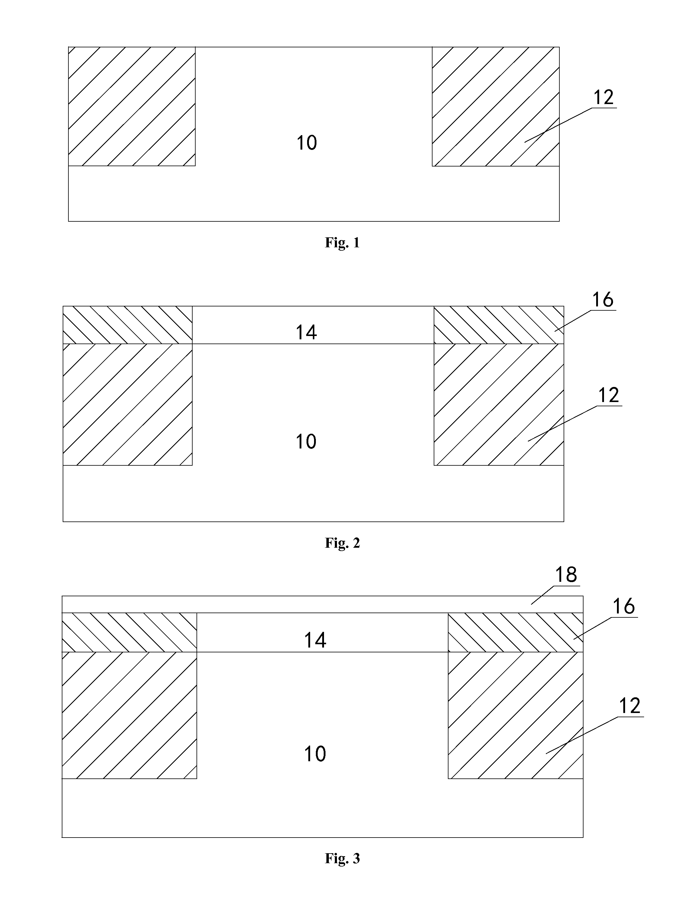
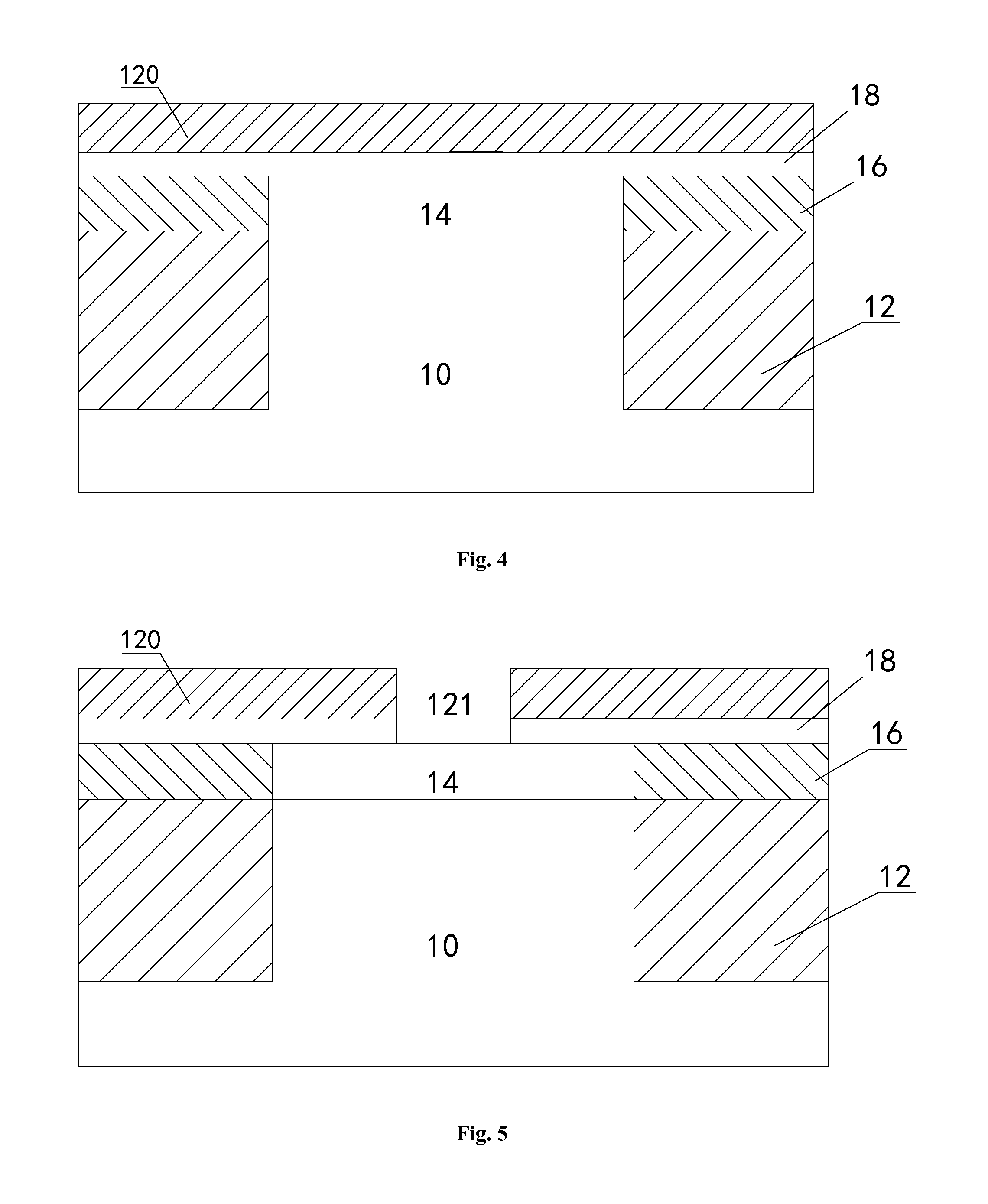
[0062]Hereinbelow, the present invention will be described in detail with reference to the attached drawings and preferred embodiments thereof.

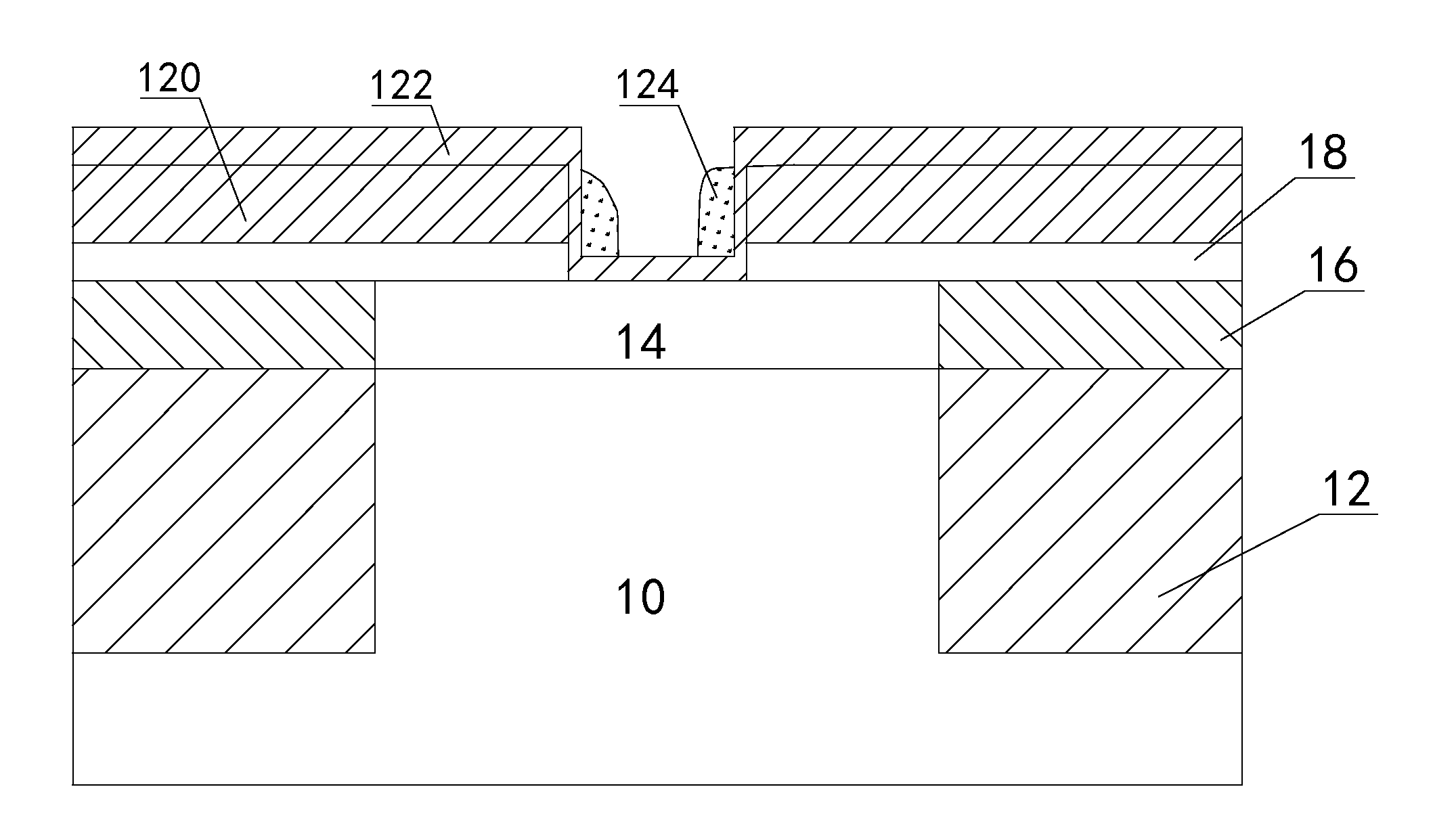
[0063]A metal silicide self-aligned SiGe heterojunction bipolar transistor of the present invention mainly comprises Si collector region, local dielectric region, base region, base-region low-resistance metal silicide layer, polysilicon emitter region, emitter-base spacer dielectric region, monocrystalline emitter region beneath emitter window enclosed by the emitter-base spacer dielectric region, contact hole dielectric layer, emitter metal electrode and base metal electrode. The emitter-base spacer dielectric region is composed of a liner silicon oxide layer and a silicon nitride inner sidewall, and the base-region low-resistance metal silicide layer extends all the way to the outside of the emitter-base spacer dielectric region.

[0064]The metal silicide self-aligned SiGe heterojunction bipolar transistor of the present invention mainly has ...


PUM


Abstract

The present invention discloses a metal silicide self-aligned SiGe heterojunction bipolar transistor, which is designed to overcome the shortcomings such as the large base resistance RB of the prior art products. The metal silicide self-aligned SiGe heterojunction bipolar transistor of the present invention mainly comprises an Si collector region, a local dielectric region, a base region, a base-region low-resistance metal silicide layer, a polysilicon emitter region, an emitter-base spacer dielectric region composed of a liner silicon oxide layer and a silicon nitride inner sidewall, a monocrystalline emitter region, a contact hole dielectric layer, an emitter metal electrode and a base metal electrode. The base-region low-resistance metal silicide layer extends all the way to the outside of the emitter-base spacer dielectric region. The present invention discloses a method of forming a metal silicide self-aligned SiGe heterojunction bipolar transistor, which is used to form the aforesaid bipolar transistor. The metal silicide self-aligned SiGe heterojunction bipolar transistor and the method of forming the same of the present invention can reduce the base resistance RB, and feature a simple process and a low cost.

Description

BACKGROUND OF THE INVENTION[0001]1. Technical Field[0002]The present invention relates to a metal silicide self-aligned SiGe heterojunction bipolar transistor and a method of forming the same.[0003]2. Description of Related Art[0004]Planar silicon (Si) bipolar transistors are conventional devices for constructing analog integrated circuits (ICs). However, because silicon materials are inherently disadvantageous in speed, group III-V compound (e.g., gallium arsenide) semiconductor devices have always dominated in the field of high-frequency and high-speed applications in the history. For SiGe heterojunction bipolar transistors obtained by introducing narrow-bandgap SiGe alloys into silicon bipolar transistors as materials of base regions, not only the high-frequency performance is improved significantly but also the advantage of the low cost of the silicon-based technology is maintained. Therefore, the SiGe heterojunction bipolar transistors have been widely used in the field of radi...

Claims


Application Information

Patent Timeline
IPC IPC(8): H01L21/331H01L29/737
CPCH01L29/7378H01L29/66242H01L29/66318
Inventor FU, JUNWANG, YU-DONGZHANG, WEILI, GAO-QINGWU, ZHENG-LICUI, JIEZHAO, YUELIU, ZHI-HONG
Owner TSINGHUA UNIV
Why Eureka
Try Eureka