

Wien filter and electron-optics apparatus
a technology of electron optics and filter, applied in the field ofwien filters, can solve problems such as adverse effects on optical characteristics, and achieve the effect of heightened magnetic shielding
- Summary
- Abstract
- Description
- Claims
- Application Information
AI Technical Summary
Benefits of technology
Problems solved by technology
Method used
Image

Examples
Embodiment Construction
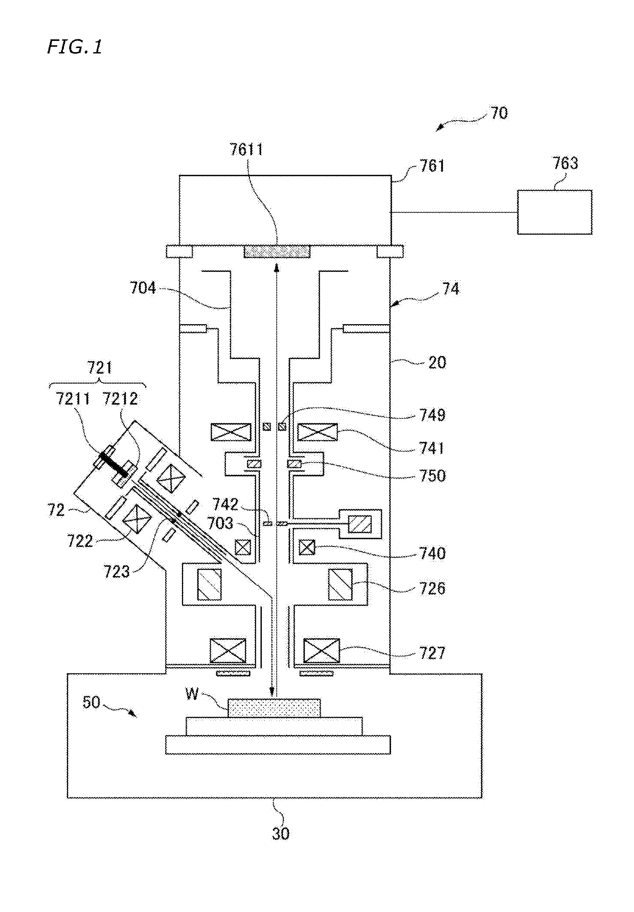
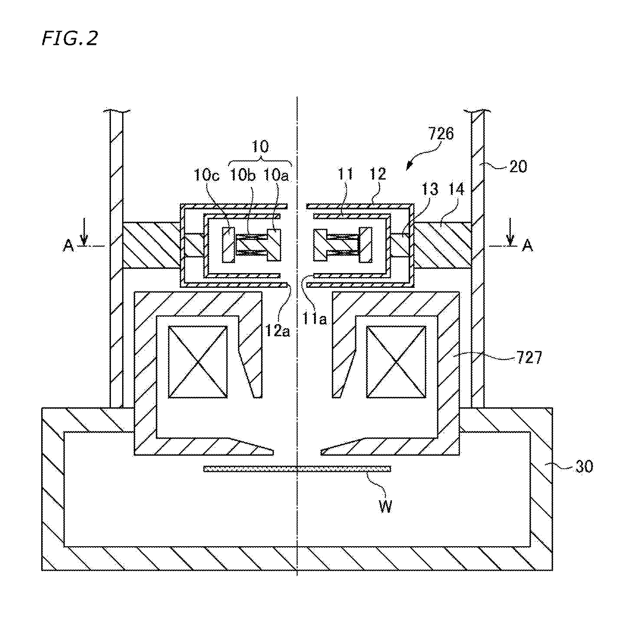
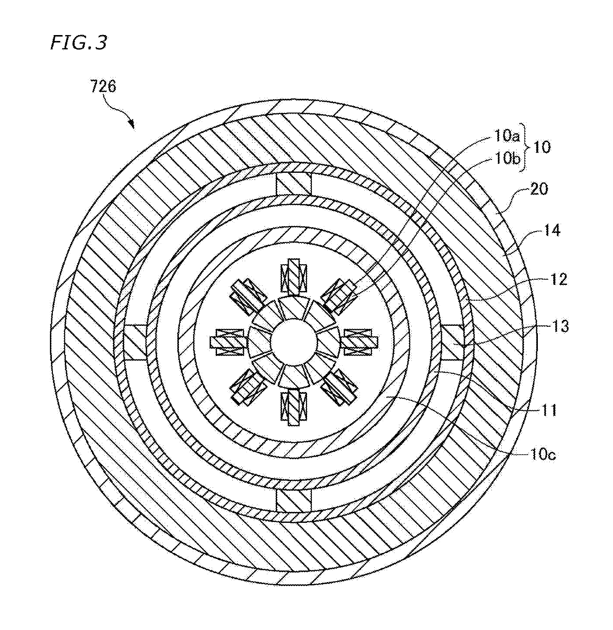
[0020]A Wien filter according to a first aspect of an embodiment is a Wien filter to be disposed inside a lens barrel made of a magnetic material, including:
[0021]a plurality of electromagnetic poles disposed at equal angular intervals about a center axis of the lens barrel;
[0022]a first magnetic shield disposed so as to cover the area around the plurality of electromagnetic poles; and
[0023]a second magnetic shield disposed so as to cover the area around the first magnetic shield, wherein
[0024]the first magnetic shield is supported by a first support member made of a non-magnetic material provided at an inner surface of the second magnetic shield, and
[0025]the second magnetic shield is supported by a second support member made of a magnetic material provided at an inner surface of the lens barrel.
[0026]According to this aspect, since the first magnetic shield is disposed so as to cover the area around the plurality of electromagnetic poles, a desired magnetic field can be stably for...
PUM
 Abstract
Description
Claims
Application Information