Semi-supervised anomaly detection in scanning electron microscope images

a scanning electron microscope and anomaly detection technology, applied in the field of images, can solve the problems of affecting the electrical parameters of the device, the operation of the semiconductor manufacturing process closer to the limitation of the performance capability of the process, and the failure to detect defects of decreasing siz

Active Publication Date: 2019-09-19
KLA TENCOR TECH CORP
View PDF0 Cites 36 Cited by
  • Summary
  • Abstract
  • Description
  • Claims
  • Application Information

AI Technical Summary

Benefits of technology

[0011]A system is provided in a first embodiment. The system comprises a wafer inspection tool and a processor in electronic communication with the wafer inspection tool. The wafer inspection tool is configured to generate images of a wafer, and includes an electron beam source and a detector. The processor operates a model configured to find one or more anomalies in the image. The model is trained using semi-supervised machine learning based on only defect-free training images of semiconductor devices.

Problems solved by technology

However, as the dimensions of semiconductor devices decrease, inspection becomes even more important to the successful manufacture of acceptable semiconductor devices because smaller defects can cause the devices to fail.
For instance, as the dimensions of semiconductor devices decrease, detection of defects of decreasing size has become necessary since even relatively small defects may cause unwanted aberrations in the semiconductor devices.
As design rules shrink, however, semiconductor manufacturing processes may be operating closer to the limitation on the performance capability of the processes.
In addition, smaller defects can have an impact on the electrical parameters of the device as the design rules shrink, which drives more sensitive inspections.
As design rules shrink, the population of potentially yield-relevant defects detected by inspection grows dramatically, and the population of nuisance defects detected by inspection also increases dramatically.
Therefore, more defects may be detected on the wafers, and correcting the processes to eliminate all of the defects may be difficult and expensive.
Furthermore, at smaller design rules, process induced failures, in some cases, tend to be systematic.
That is, process-induced failures tend to fail at predetermined design patterns often repeated many times within the design.
There is learning involved in the system, but it tends to happen in an ad hoc manner and at a high level in a loop typically involving an SEM review where the results of the inspection are deemed as true defects, false alarms, nuisance, etc.
The relationships between process-related causes and an operator's ability to observe the effects are so complex that conventional methods do not lend themselves to converging on recipes that take full advantage of the raw capability of the inspection equipment used to control the semiconductor manufacturing process.
This is a manual technique, which is tedious and prone to errors.
Visual review by an operator can be time-consuming.
Like the other previous technique, this is a partially manual technique, which is tedious and prone to errors.
The annotation process tends to be difficult because of the small and subtle characteristic of the defects.
This creates unexpected error behavior during the anomaly detection.
An operator needed to find anomaly patterns in a huge population of nominal patterns, which can be challenging.

Method used


Image

  • Semi-supervised anomaly detection in scanning electron microscope images
  • Semi-supervised anomaly detection in scanning electron microscope images
  • Semi-supervised anomaly detection in scanning electron microscope images

Examples


first embodiment

[0062]In a first embodiment, outliers can be determined using distance in a feature space. Some machine learning feature vectors are extracted from the defect-free training images. When new images are passed in during a test job run, the same types of feature vectors can be extracted from these new images. How far a feature vector of one new image is from the feature vectors of all defect-free training images can be determined. If the distance exceeds a threshold, then the new image is considered an outlier. For example, a center of mass for the image dataset in the defect-free training data can be determined. The distance between the new image and this center of mass can be determined, which can be used to find outliers.

second embodiment

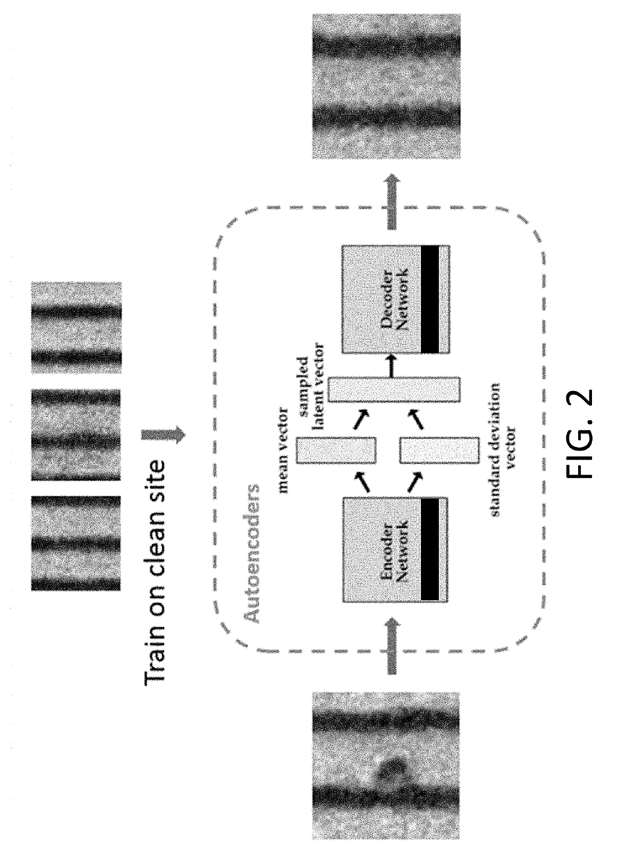
[0063]In a second embodiment, outliers can be determined using a GAN with one CNN as its discriminatory network. A GAN is composed of two networks: a generator network followed by a discriminator network. The autoencoder can be used as the generator and the CNN can be used as the discriminator. All training images for autoencoder may be nominal (i.e., defect-free). Reconstruct images can be generated by this autoencoder using these training images as examples. Some look more real (like nominal images) and some look more fake (like anomaly images). The job of the discriminator is to determine from these generated images which are real and which are fake. After the training finishes, the discriminator network will have the ability to determine which image is nominal (real) while which is anomaly (fake). Thus, the new images (test images) can be passed to the CNN discriminator network to find out if the images are anomaly or not. In this way, GAN can be used to find outliers in new dat...


PUM


Abstract

Autoencoder-based, semi-supervised approaches are used for anomaly detection. Defects on semiconductor wafers can be discovered using these approaches. The model can include a variational autoencoder, such as a one that includes ladder networks. Defect-free or clean images can be used to train the model that is later used to discover defects or other anomalies.

Description

CROSS-REFERENCE TO RELATED APPLICATIONS[0001]This application claims priority to the provisional patent application filed Mar. 19, 2018 and assigned U.S. App. No. 62 / 644,962, the disclosure of which is hereby incorporated by reference.FIELD OF THE DISCLOSURE[0002]This disclosure relates to anomaly detection in images and, more particularly, to anomaly detection in scanning electron microscope images of semiconductor wafers.BACKGROUND OF THE DISCLOSURE[0003]Evolution of the semiconductor manufacturing industry is placing ever greater demands on yield management and, in particular, on metrology and inspection systems. Critical dimensions continue to shrink, yet the industry needs to decrease time for achieving high-yield, high-value production. Minimizing the total time from detecting a yield problem to fixing it determines the return-on-investment for a semiconductor manufacturer.[0004]Fabricating semiconductor devices, such as logic and memory devices, typically includes processing ...

Claims


Application Information

Patent Timeline
Patent Type & Authority Applications(United States)
IPC IPC(8): G06T7/00G06V10/764
CPCG06T7/001G06T2207/20081G06N3/04G06T2207/30148G06T2207/10061G06T2207/20084G06T7/0004G06V10/764G06V10/82G06N3/08H01L21/67242H01L22/12H01L22/24G06N3/088G06N3/047G06N3/045H01L22/30
Inventor LU, SHAOYUHE, LIVENKATARAMAN, SANKAR
Owner KLA TENCOR TECH CORP
Why Eureka
Try Eureka