Method of manufacturing light emitting module, and light emitting module

a technology of light emitting modules and manufacturing methods, applied in the direction of instruments, optical elements, optics, etc., can solve the problems of insufficient thickness reduction, inability to use in applications which require light emission characteristics with little luminance non-uniformity, and insufficient thickness reduction. , to achieve the effect of light emission characteristics, little luminance non-uniformity, and reduced thickness

Active Publication Date: 2019-09-26
NICHIA CORP
View PDF0 Cites 40 Cited by
  • Summary
  • Abstract
  • Description
  • Claims
  • Application Information

AI Technical Summary

Benefits of technology

[0009]The method of manufacturing a light emitting module can provide a light emitting module including a light guiding plate and a light emitting element, the light emitting module attaining uniform light emission with little luminance non-uniformity while having a reduced thickness as a whole. This is because a light adjustment portion is bonded to a recess of the light guiding plate, and a light emitting element unit in which the light emitting element is bonded to the light adjustment portion is disposed at a predetermined position on the light guiding plate. Further, the method of manufacturing a light emitting module has such a feature that the light emitting element unit includes the fluorescent material-containing light adjustment portion and the light emitting element as an integral structure, and the light adjustment portion of the light emitting element unit is bonded to the recess of the light guiding plate to dispose the light emitting element unit at a predetermined position on the light guiding plate. The light emitting element unit is bonded at a predetermined position with high accuracy with less relative positional deviation of the light adjustment portion, the light emitting element and the recess of the light guiding plate, so that light emitting modules having a reduced thickness as a whole can be efficiently mass-produced, and luminance non-uniformity of a surface of the light guiding plate can be reduced.
[0011]The light emitting module has such a feature that a light emitting element unit a fluorescent material-containing light adjustment portion is bonded to a light emission surface of a light emitting element is bonded to a recess of a light guiding plate. Furthermore, the outline of an insertion portion of the light emitting element unit, which is disposed in the recess, is smaller in size than the inner shape of the recess of the light guiding plate, and a bonding wall formed using a light-transmissive bonding agent supplied in a ring gap formed between the insertion portion and the recess. This can allow the light emitting module to have light emission characteristics with little luminance non-uniformity and to have reduced thickness as a whole. This is because the insertion portion of the light emitting element unit is disposed in the recess of the light guiding plate, the light-transmissive bonding wall is provided between the insertion portion of the light emitting element unit and the recess, and the light emitting element unit is accurately disposed at a predetermined position in the recess of the light guiding plate, so that light emitted from the light emitting element can enter into the light guiding plate through the light adjustment portion, be diffused at the light guiding plate, and exit outside.

Problems solved by technology

However, in the light source device disclosed in JP2015-32373A, the distance between the mounting substrate and the diffusion plate should be greater than the thickness of the lens member, so that there is a possibility to fail sufficient thickness reduction.
In addition, the light source device in JP2016-115703A cannot uniformly disperse and irradiate light from a plurality of light emitting elements, and thus cannot be used in applications which require light emission characteristics with little luminance non-uniformity.

Method used


Image

  • Method of manufacturing light emitting module, and light emitting module
  • Method of manufacturing light emitting module, and light emitting module
  • Method of manufacturing light emitting module, and light emitting module

Examples


Embodiment Construction

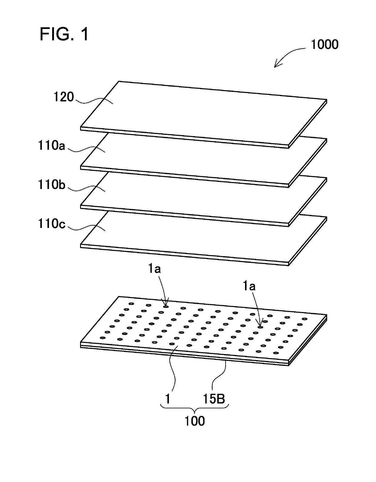
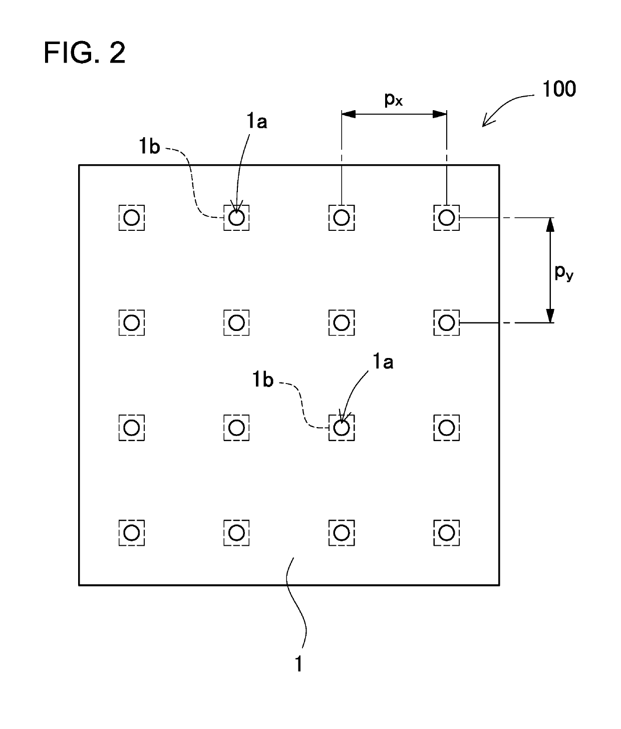
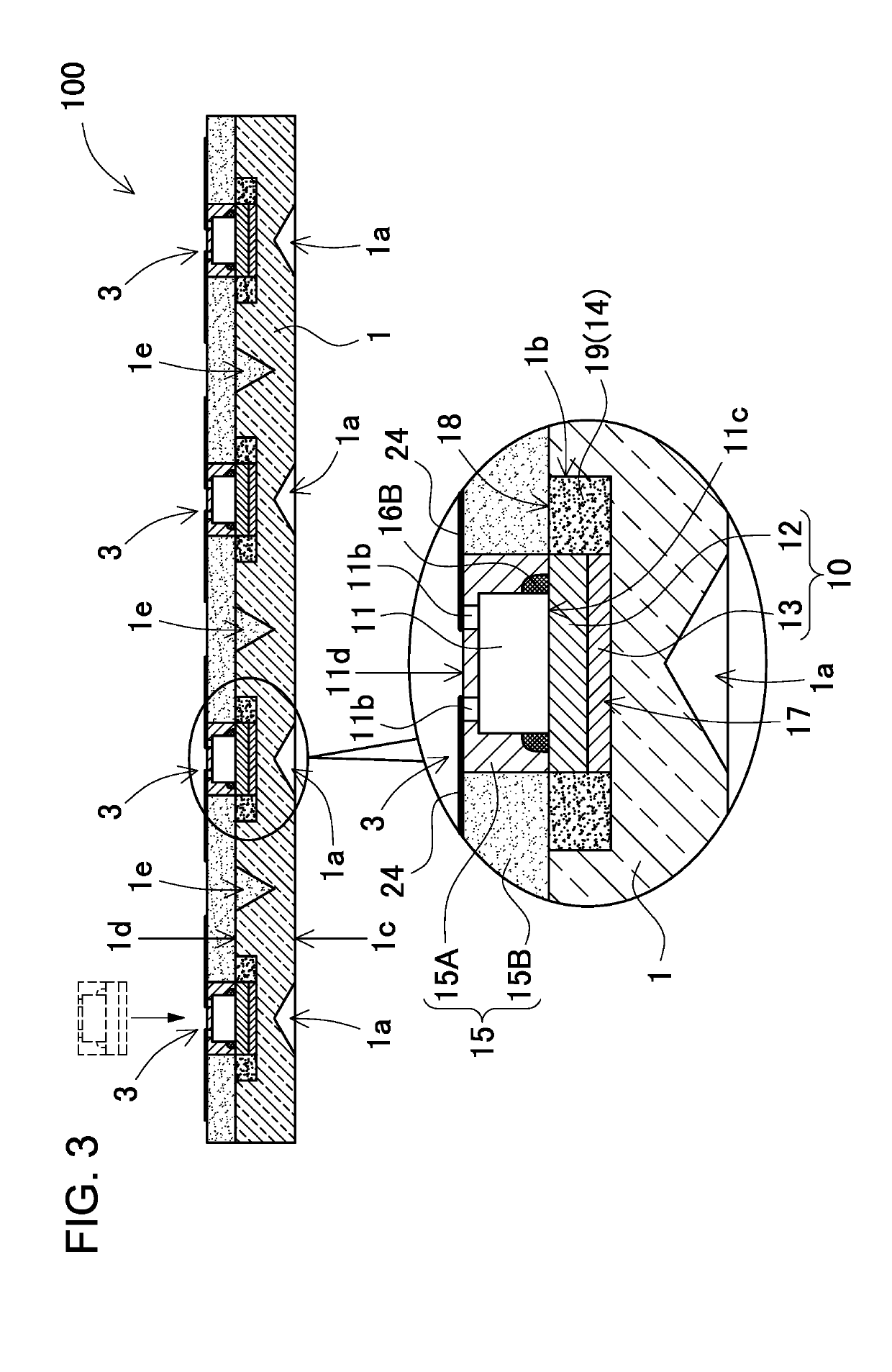
[0025]Hereinafter, the present disclosure will be described in detail with reference to the drawings. In the following descriptions, terms showing a specific direction or position (e.g. “upper”, “lower” and other terms relating to such terms) are used as necessary, but these terms are used for ease of understanding of the disclosure by referring to the drawings, and the meaning of these terms does not limit the technical scope of the present disclosure. In the following description, in principle, identical name and reference character denote an identical or similar member.

[0026]Further, embodiments described below are intended to give an example of a light emitting module and a method of manufacturing the light emitting module for embodying the technical idea of the present disclosure, and do not limit the present disclosure to the following embodiments. In addition, unless otherwise specified, the dimensions, materials, shapes, relative arrangements and so on of components describe...


PUM

PropertyMeasurementUnit
thicknessaaaaaaaaaa
thicknessaaaaaaaaaa
sizeaaaaaaaaaa

Abstract

The method of manufacturing a light emitting module includes: providing a light guiding plate having a first main surface serving as a light emitting surface; and a second main surface positioned opposite to the first main surface and provided with a recess; providing a light adjustment portion containing a fluorescent material; providing a light emitting element unit in which a light emitting element comprising an electrode is integrally bonded to the light adjustment portion; bonding the light adjustment portion of the light emitting element unit to the recess; and forming wiring on the electrode of the light emitting element.

Description

CROSS-REFERENCE TO RELATED APPLICATION[0001]This application claims priority to Japanese Patent Application No. 2018-059064, filed on Mar. 26, 2018, and Japanese Patent Application No. 2019-056065 filed on Mar. 25, 2019, the disclosures of which are hereby incorporated by reference in their entirety.BACKGROUND1. Field of the Invention[0002]The present disclosure relates to a method of manufacturing a light emitting module, and a light emitting module.2. Description of the Related Art[0003]Light emitting devices using light emitting elements such as light emitting diodes are widely used as light sources of backlights for liquid crystal displays, and various light sources for displays.[0004]For example, a light source device as disclosed in Japanese Patent Publication No. 2015-32373A includes a plurality of light emitting elements mounted on a mounting substrate, hemispherical lens members each encapsulating the light emitting elements, and a light diffusion member to which light from...

Claims


Application Information

Patent Timeline
Patent Type & Authority Applications(United States)
IPC IPC(8): G02F1/1335H01L25/075H01L33/36H01L33/50H01L33/62H01L33/56
CPCG02F1/133611G02F1/133603H01L2933/0066H01L33/32H01L25/0753H01L33/36G02F2001/133612H01L33/507H01L2933/0041H01L2933/005G02F2001/133614H01L33/62H01L33/56G02F1/133606H01L33/58H01L2933/0058G02F1/133601G02F1/133614G02F1/133607G02B6/0023G02B6/0021G02F1/133612
Inventor HASHIMOTO, TORU
Owner NICHIA CORP
Why Eureka
Try Eureka