Method of processing wafer

Active Publication Date: 2019-10-24
DISCO CORP
View PDF0 Cites 1 Cited by
  • Summary
  • Abstract
  • Description
  • Claims
  • Application Information

AI Technical Summary

Benefits of technology

This patent describes a way to cool down a wafer with a metal film using a contact cooling means. By efficiently cooling the entire surface of the wafer, the metal film becomes easier to break down. This makes it possible to divide the wafer into individual device chips without causing any damage to the metal film and ensuring that the devices on the chips work properly.

Problems solved by technology

Since a metal film is ductile or tenacious, when a wafer with such a metal film is divided by one of the methods referred to above, the metal film may be elongated and remain unbroken, or may be broken but produce large burrs that tend to make devices on the wafer defective.
With this arrangement, since the entire upper surface of the wafer is efficiently cooled by the contact surface of the contact cooling means, the metal film loses its ductility and develops low-temperature brittleness.

Method used


Image

  • Method of processing wafer
  • Method of processing wafer
  • Method of processing wafer

Examples


Embodiment Construction

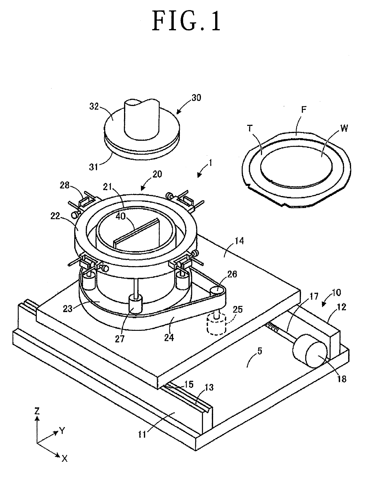
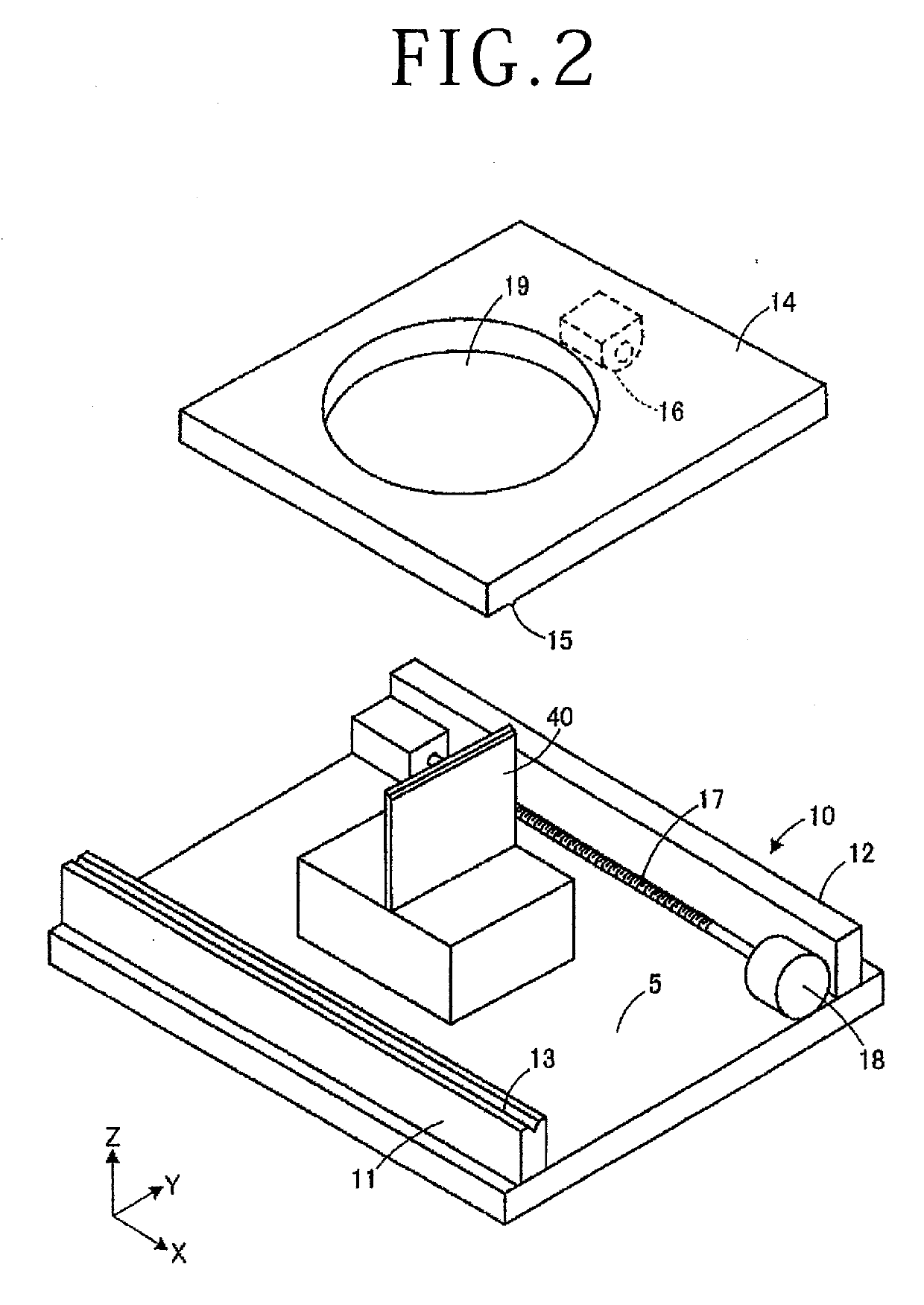
[0013]A wafer dividing apparatus for carrying out a method of processing a wafer, or a wafer processing method, according to an embodiment of the present invention will be described in detail below with reference to the accompanying drawings. FIG. 1 is a perspective view of the wafer dividing apparatus according to the present embodiment. FIG. 2 is an exploded perspective view of a portion of the wafer dividing apparatus illustrated in FIG. 1. The wafer dividing apparatus illustrated in FIGS. 1 and 2 is by way of example only, and may be changed or modified.

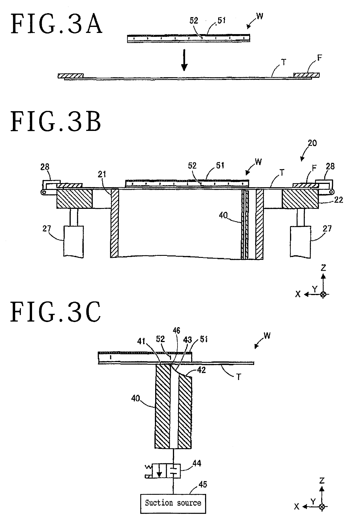
[0014]As illustrated in FIG. 1, a wafer dividing apparatus, denoted by 1, is arranged to divide a wafer W held on a holding table 20 into individual device chips along a grid of projected dicing lines on the wafer W by applying suction forces to the projected dicing lines where the mechanical strength of the wafer W is reduced. The projected dicing lines that are formed on a face side of the wafer W demarcate the face side of the...


PUM


Abstract

A method of processing a wafer with a metal film to divide the wafer into individual device chips along a grid of projected dicing lines where the mechanical strength of the wafer is reduced. The method includes the steps of sticking a holding tape to a face side of the wafer, holding the wafer while a reverse side of the wafer with the metal film thereon is being exposed, and drawing the wafer under suction along the projected dicing lines to fracture the wafer along the projected dicing lines while the reverse side of the wafer is being cooled in its entirety.

Description

BACKGROUND OF THE INVENTIONField of the Invention[0001]The present invention relates to a method of processing a wafer to divide the wafer into a plurality of device chips.Description of the Related Art[0002]There has been proposed a method of dividing a wafer such as a semiconductor wafer or the like by forming severance initiating points with reduced mechanical strength in the wafer along projected dicing lines thereon and applying an external force to the wafer to separate the wafer into a plurality of device chips along the projected dicing lines. The external force may be applied in various ways. For example, if a wafer with a small chip size, or a wafer with a large thickness, or a wafer with a relatively large hardness is to be divided, then it is customary to divide the wafer by locally pressing the wafer or pulling down the wafer under suction along the projected dicing lines (see, for example, Japanese Patent Laid-Open No. 2012-146744 and Japanese Patent Laid-Open No. 2006...

Claims


Application Information

Patent Timeline
IPC IPC(8): H01L21/78H01L21/67H01L21/304
CPCH01L21/78H01L21/304H01L21/67092H01L21/67132H01L21/6838
Inventor ZHAO, JINYAN
Owner DISCO CORP
Why Eureka
Try Eureka