Flexible substrate, manufacturing method thereof and touch display panel

Inactive Publication Date: 2019-11-14
SHENZHEN CHINA STAR OPTOELECTRONICS SEMICON DISPLAY TECH CO LTD
View PDF3 Cites 2 Cited by
  • Summary
  • Abstract
  • Description
  • Claims
  • Application Information

AI Technical Summary

Benefits of technology

[0025]The implementation of the present invention possesses the following results: the flexible substrate and the touch display panel provided by the present invention do not need to separately integrate the touch circuit on the outer side of the flexible substrate, thus inevitably increasing the thickness of the entire touch display panel. By simply integrating the touch circuit in the flexible substrate layer, the thickness of the fle

Problems solved by technology

All three technologies will lose the panel y

Method used


Image

  • Flexible substrate, manufacturing method thereof and touch display panel
  • Flexible substrate, manufacturing method thereof and touch display panel

Examples


Example

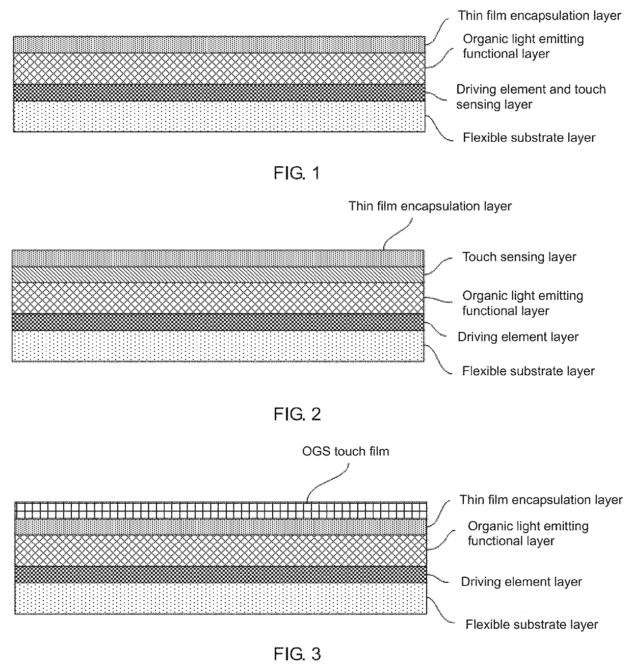
[0034]The present invention provides a flexible substrate. The flexible substrate comprises at least two flexible substrate layers and a touch circuit disposed between the at least two flexible substrate layers. For instance, in one embodiment as shown in FIG. 4, the flexible substrate comprises a first flexible substrate layer 11 and a second flexible substrate layer 12, and the touch circuit 13 is arranged between the first flexible substrate layer 11 and the second flexible substrate layer 12.

[0035]The touch circuit is a self-capacitive touch circuit or a mutual-capacitive touch circuit, and the self-capacitive touch circuit comprises a touch electrode layer, and the mutual-capacitive touch circuit comprises two touch electrode layers.

[0036]Furthermore, as shown in FIG. 5, as the touch circuit is the self-capacitive touch circuit, the at least two flexible substrate layers comprise a first flexible substrate layer 11 and a second flexible substrate layer 12, and the touch electro...


PUM


Abstract

Provided are a flexible substrate, a manufacturing method thereof and a touch display panel. The touch display panel includes a flexible substrate, a driving element layer, an organic light emitting functional layer and thin film encapsulation layer located on the flexible substrate. The flexible substrate includes at least two flexible substrate layers and a touch circuit disposed between the at least two flexible substrate layers. A thickness of the touch display panel can be reduced to improve a production yield of the touch display panel.

Description

CROSS-REFERENCE TO RELATED APPLICATION[0001]This application is a continuing application of PCT Patent Application No. PCT / CN2018 / 092350 entitled “Flexible substrate, manufacturing method thereof and touch display panel”, filed on Jun. 22, 2018, which claims priority to Chinese Patent Application No. 201810458414.7, filed on May 14, 2018, both of which are hereby incorporated in its entireties by reference.FIELD OF THE INVENTION[0002]The present invention relates to a display field, and more particularly to a flexible substrate, a manufacturing method thereof and a touch display panel.BACKGROUND OF THE INVENTION[0003]As a new generation display technology, AMOLED (Active-matrix organic light emitting diode) display panel has low power consumption, high color gamut, high brightness, high resolution, wide viewing angle and high response speed. The advantages are therefore highly favored by the market. The flexible AMOLED display panel even has the advantages of being curled, folded an...

Claims


Application Information

Patent Timeline
IPC IPC(8): H01L27/32H01L51/00H01L51/56G06F3/044G06F3/041
CPCH01L51/56G06F3/044G06F2203/04102H01L51/0097H01L27/323G06F2203/04103G06F3/0412G06F3/0443G06F3/0445Y02E10/549H10K59/40H10K77/111H10K71/00
Inventor XU, XIANGYANG
Owner SHENZHEN CHINA STAR OPTOELECTRONICS SEMICON DISPLAY TECH CO LTD
Why Eureka
Try Eureka