Organic Light Emitting Diode Display Panel and Method for Encapsulating Same

a light-emitting diode and display panel technology, applied in the field of display technology, can solve the problems of high maintenance cost, damage to the mask surface, and damage to the mask, and achieve the effect of reducing production and maintenance costs, easy peeling of organic peeling, and simple encapsulation process

Active Publication Date: 2019-11-28
WUHAN CHINA STAR OPTOELECTRONICS SEMICON DISPLAY TECH CO LTD
View PDF6 Cites 7 Cited by
  • Summary
  • Abstract
  • Description
  • Claims
  • Application Information

AI Technical Summary

Benefits of technology

[0023]Advantageous effects of the disclosure are as follows. This disclosure relates to the organic light emitting diode display panel and the encapsulation method of the organic light emitting diode display panel. An easily peelable organic peeling layer is formed on a predetermined area on a surface of an array substrate by a thermal evaporation method. A Thin film encapsulation is performed directly on the organic peeling layer and an OLED display panel layer through a full-surface coating method without using a mask. Moreover, thin film encapsulation layers disposed on an interval area between celled display panels are removed by a stripping process of peeling the organic peeling layer. Thus, the mask is not necessary to be used during the encapsulation method. The full-surface coating method can be adopted in a PECVD, ALD, PLD and other methods. A process of the encapsulation method is simple and avoids problems such as damage to the mask and difficulty in cleaning, and reduces production and maintenance costs.
of the disclosure are as follows. This disclosure relates to the organic light emitting diode display panel and the encapsulation method of the organic light emitting diode display panel. An easily peelable organic peeling layer is formed on a predetermined area on a surface of an array substrate by a thermal evaporation method. A Thin film encapsulation is performed directly on the organic peeling layer and an OLED display panel layer through a full-surface coating method without using a mask. Moreover, thin film encapsulation layers disposed on an interval area between celled display panels are removed by a stripping process of peeling the organic peeling layer. Thus, the mask is not necessary to be used during the encapsulation method. The full-surface coating method can be adopted in a PECVD, ALD, PLD and other methods. A process of the encapsulation method is simple and avoids problems such as damage to the mask and difficulty in cleaning, and reduces production and maintenance costs.

Problems solved by technology

In the PECVD method, if a surface of the mask is contaminated by foreign matter and is not cleaned in time, arcing may occur under a reaction of positive and negative electric fields, thereby causing damage to the mask.
Simultaneously, the surface of the mask may be damaged due to plasma erosion.
The mask needs to be replaced on time and that causes high maintenance costs.
For the methods such as ALD and PLD, since a self-cleaning function is not provided, the surface of the mask will gradually accumulate depositions of film layers with over time, and the deposited film layer is difficult to clean, thereby causing overall higher costs.

Method used


Image

  • Organic Light Emitting Diode Display Panel and Method for Encapsulating Same
  • Organic Light Emitting Diode Display Panel and Method for Encapsulating Same
  • Organic Light Emitting Diode Display Panel and Method for Encapsulating Same

Examples


first embodiment

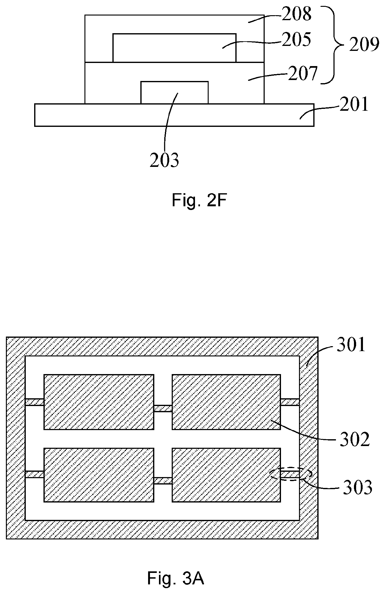
[0045]Specifically, referring to FIGS. 3A-3B, structural schematic views of the mask plate for preparing an organic peeling layer according to this disclosure are shown. The mask plate comprises a mask frame 301 and at least a first mask portion 302 disposed within the mask frame 301. The first mask portion 302 is connected to the mask frame 301 via a second mask portion 303, and the second mask portion 303 is interval disposed in a corresponding organic peeling layer region corresponding to the organic peeling layer. In the embodiment, in the thermal evaporation process, the thermal evaporation process of the organic peeling layer is performed using two mask plates respectively. The structural schematic view of a first mask plate is shown in FIG. 3A. A hollow region is used for evaporating the organic peeling layer, and each of the first mask portions 302 is configured to block a thin film encapsulation layer region set on the corresponding OLED display panel, and the second mask p...

second embodiment

[0046]Referring to FIG. 4, a structural schematic view of a mask plate for preparing an organic peeling layer according to this disclosure is shown. The mask plate includes a mask frame 401, a first mask portion 402, and a second mask portion 403. The difference between this embodiment and the above embodiment is that: in the thermal evaporation process of the embodiment, the thermal evaporation process is performed two times by a same mask plate, and any one of the second mask portions 403 is disposed completely corresponding to one side of a center line of the first mask portion 402. The second mask portion 403 connected with a center line direction of the first mask portion 402 is located at both sides of the center line. After a first thermal evaporation process is completed, the mask plate is rotated 180° and then a second thermal evaporation process is performed. Since a position of the second mask portion 403 of the mask plate corresponding to the substrate in the first therm...


PUM


Abstract

An organic light emitting diode (OLED) display panel and a encapsulation method of the organic light emitting diode display panel are provided. The encapsulation method includes steps of providing an OLED display panel having an OLED light emitting element layer in a display area thereof and an organic peeling layer in a non-display area thereof; laminating an inorganic film layer prepared in a full-surface coating method and an organic film layer only covering the display area sequentially; and peeling off the organic peeling layer together with the inorganic film layer on the surface of the organic peeling layer, so as to form a thin film encapsulation layer.

Description

FIELD OF INVENTION[0001]This disclosure relates to display technology, and more particularly to an organic light emitting diode display panel and a encapsulation method of the organic light emitting diode display panel. encapsulationBACKGROUND OF INVENTION[0002]A flexible organic light emitting diode (OLED) display is suitable for application in wearable display devices due to low energy consumption, bendability, and other characteristics. The flexible OLED display is a popular technology for display industry. Generally, a thin film encapsulation design of the flexible OLED display panel generally uses an organic / inorganic film layer overlap structure to achieve water and oxygen blocking, foreign matter blocking, and stress release.[0003]At present, one method of preparing the inorganic film layer in a thin film encapsulation process is generally performed by plasma enhanced chemical vapor deposition (PECVD), atomic layer deposition (ALD) or pulsed laser deposition (PLD), and other ...

Claims


Application Information

Patent Timeline
Patent Type & Authority Applications(United States)
IPC IPC(8): H01L51/52H01L51/56
CPCH01L51/5256H01L51/56H10K50/8445H10K71/00
Inventor WANG, KANWANG, JUNYUANHSU, HSIANGLUN
Owner WUHAN CHINA STAR OPTOELECTRONICS SEMICON DISPLAY TECH CO LTD
Why Eureka
Try Eureka