Method for forming mirror-reflecting film in optical wiring board, and optical wiring board

a technology of optical wiring board and mirror-reflecting film, which is applied in the direction of optical elements, circuit optical details, instruments, etc., can solve the problems of increased material costs, difficult adhesion task, and excessive economic burden, and achieve the effect of easy peeling

Active Publication Date: 2011-10-06
PANASONIC CORP
View PDF3 Cites 6 Cited by
  • Summary
  • Abstract
  • Description
  • Claims
  • Application Information

AI Technical Summary

Benefits of technology

[0033]A characteristic of the present invention is that, in a well-known process of fabricating an optical wiring board such as for example that shown in FIG. 1 above, an innovation has been made in the method of formation of the mirror-reflecting film in particular. Specifically, as explained in detail below, the invention is characterized in that a multilayer film in which a base, a metal layer and an adhesive layer are layered in this order is used; the multilayer film is set such that the adhesive layer is in contact with an inclined face for a mirror which is formed on the waveguide in the optical wiring board; and thereafter the base alone is peeled to cause transfer and bonding of the metal layer to the inclined face for the mirror.
[0034]FIG. 2 shows the configuration of the multilayer film for transfer, in which fundamentally a three-layer structure comprising a base A, metal layer B, and adhesive layer C is employed.
[0035]No limitations in particular are imposed on the material of the base A, and a polyester resin such as polyethylene terephthalate (PET), an acrylic resin, a polyimide resin, and the like can be used. It is preferable that the material be easily peelable from the metal layer B with which the base is layered, and ordinary plastic film is generally appropriate.
[0036]When the adhesive layer C which is used is a material requiring heating for transfer, such as for example a thermosetting resin or a hot-melt resin, the base A can be selected from materials with thermal resistance, having the ability to withstand the heat used in transfer. No limitations in particular are imposed on the thickness of the base A, but it is preferable that the layer be thin in order to secure the flexibility to enable the base to follow the inclined face for mirror formation, and a thickness of 0.2 mm or less is recommended. The thickness of the base A is preferably in, but not limited to, a range of 0.01 to 0.05 mm.
[0037]No limitations in particular are imposed on the type of the metal layer B either, but it is preferable to use a metal having high reflectivity for the light to be transmitted. For example, 850 nm is a representative wavelength of VCSELs, which are light-emitting elements suitable for surface mounting. Metals with a high reflectivity at this wavelength are, for example, copper, silver, gold, aluminum, nickel, chromium, and similar. When the stability of the material is considered, copper, silver and gold are particularly preferable, and gold in particular is optimal. However, of course another metal can be selected, taking into consideration the environment of use including temperature and humidity, or required characteristics.
[0038]The thickness of the metal layer B need only be such that transmitted light does not penetrate, and a target thickness of approximately 0.1 μm or greater is sufficient. The thickness of the metal layer B is preferably in, but not limited to, a range of 0.1 to 0.5 μm.

Problems solved by technology

However, according to an investigation by the inventors, vacuum processing equipment or other large-scale equipment is necessary in order to perform such methods, so that excessive economic burdens are imposed.
Moreover, according to the investigation by the inventors, metal cannot be propelled only onto limited necessary areas in these methods, so that adhesion of the metal is to be performed in a state covering regions other than the regions for adhesion by masking, thus making the adhesion task difficult.
In addition, the metal evaporation source (sputtering source) is used in greater than the needed amount, so that there is the problem that material costs are increased.

Method used


Image

  • Method for forming mirror-reflecting film in optical wiring board, and optical wiring board
  • Method for forming mirror-reflecting film in optical wiring board, and optical wiring board
  • Method for forming mirror-reflecting film in optical wiring board, and optical wiring board

Examples


example 1

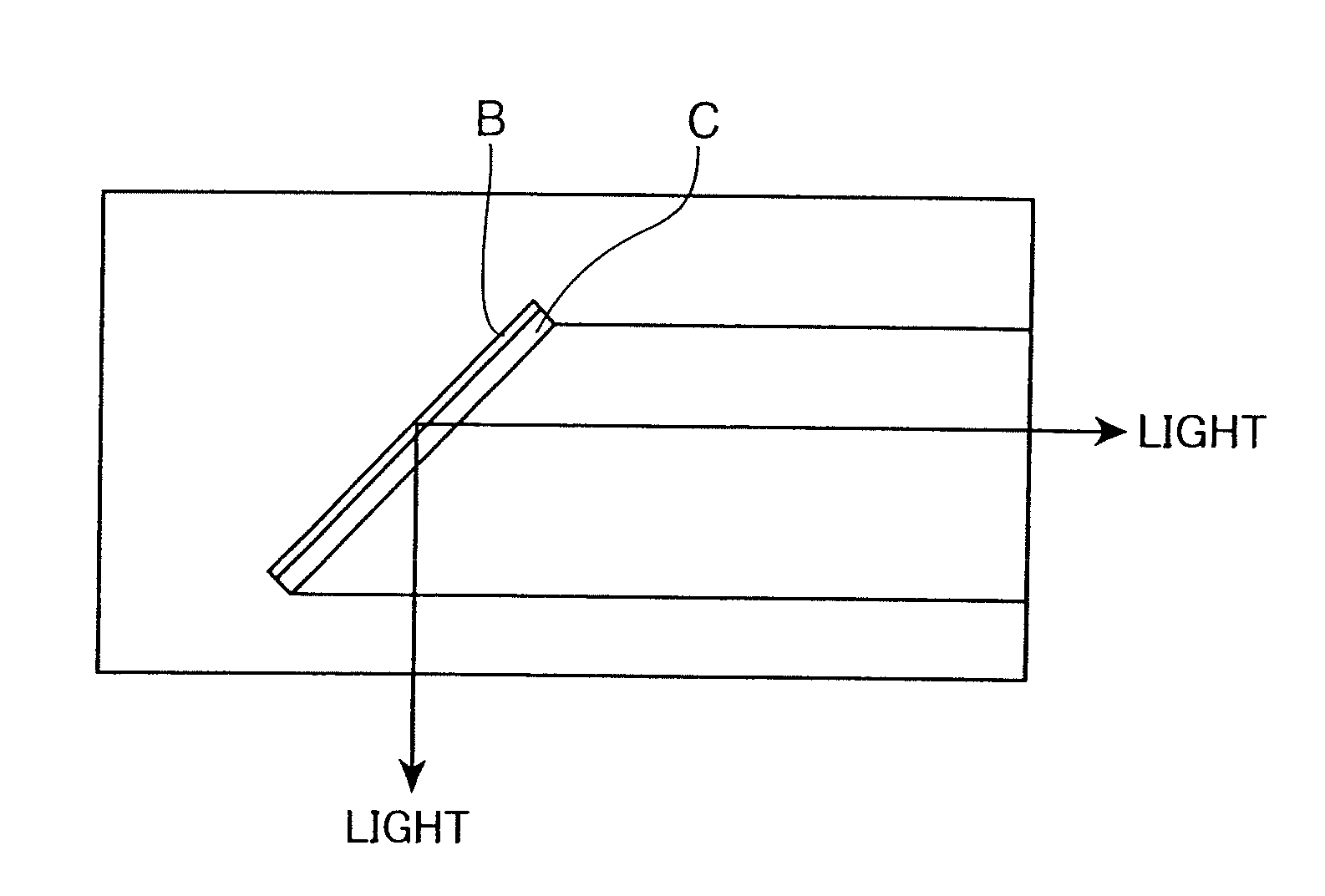
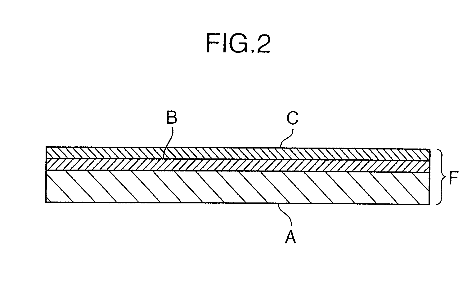
[0097]As a copper-plated flexible board, a FELIOS board, manufactured by Panasonic Electric Works Co., Ltd. (product name “R-F775”, polyimide thickness 25 μm, two-sided board) was made available, and all the Cu on one face was etched off.

[0098]As the material for cladding, the epoxy film A was used; the OPP film of the film A was peeled away, the film was placed such that the material was in contact with the etched-off face of the board, and pressure was applied at 60° C. and in 0.2 MPa for 120 seconds to perform lamination. Next, a super-high pressure mercury lamp was used for irradiation with 2000 mJ of light at 365 nm to cause hardening, and finally the PET film was peeled away to form the lower cladding on the board.

[0099]Next, the epoxy film B was used as the core material, and similarly to the above procedure, the epoxy film B was placed on the surface of the lower cladding, and lamination was performed by applying pressure at 60° C. and in 0.2 MPa for 120 seconds. Next, a pho...

example 2

[0107]Methods similar to those of Example 1 were used, up to formation of the 45° inclined faces.

[0108]Next, reflecting film formation by thermal transfer was performed. As the multilayer film for transfer, the multilayer film 3 was used, and as the head for thermal transfer, a temperature-controlled type soldering iron similar to that of Example 1 was used.

[0109]The multilayer film 3 was held with tweezers, and while using a microscope for observation, was positioned such that the side of the adhesive layer of the multilayer film 3 was in contact with the 45° inclined face obtained by dicing. The soldering iron with the tip temperature adjusted so as to be 170° C. was brought into contact for 5 seconds with the base face side of the multilayer film 3 to cause hardening of the adhesive layer. Then, upon peeling and removing the multilayer film 3, only the polyimide film was peeled from the 45° inclined face, and it was confirmed that Al was transferred and bonded to the inclined fac...

example 3

[0113]Similarly to Example 1, fabrication up to formation of the 45° inclined faces was performed.

[0114]Next, reflecting film formation by thermal transfer was performed. As the multilayer film for transfer, the multilayer film 1 was used. As the soldering iron for thermal transfer, the same temperature-controlled type soldering iron as in Example 1 was used; silicone rubber of thickness 15 μm was mounted so as to cover the tip of the iron, and a thermocouple was installed.

[0115]The multilayer film 1 was held with tweezers, and while using a microscope for observation, was positioned such that the side of the adhesive layer of the multilayer film 1 was in contact with the 45° inclined face obtained by dicing. The soldering iron, in which a tip temperature was adjusted such that the thermocouple readout was 170° C. (the silicone rubber surface was at 170° C.), was brought into contact for 5 seconds with the base face side to cause hardening of the adhesive layer. Then, upon peeling a...


PUM


Abstract

An aspect of the present invention is directed to a method for forming a mirror-reflecting film on a waveguide in an optical wiring board, characterized in that a multilayer film, in which a base, a metal layer and an adhesive layer are layered in this order, is used, and the metal layer is transferred and bonded to an inclined face for mirror-reflecting film formation provided on the waveguide, with the adhesive layer of the multilayer film intervening. The present invention provides a method which, when forming a mirror-reflecting film on a waveguide in an optical wiring board, enables inexpensive and easy formation of the mirror-reflecting film, using the smallest quantity of metal possible and employing comparatively simple facilities and techniques.

Description

TECHNICAL FIELD[0001]This invention relates to a method for forming a mirror-reflecting film in an optical wiring board, and to an optical wiring board comprising the mirror-reflecting film formed by this method.BACKGROUND ART[0002]Optical wiring boards, which are printed boards incorporating optical waveguides, are attracting attention as a means of resolving such persistent problems in various information processing equipment as high-frequency noise accompanying faster signals and inadequate transmission bandwidth.[0003]In such optical wiring boards, mirror-reflecting films are formed on optical waveguides in order to bend light at desired angles, as for example when light is output from or, conversely, input to the board surface. As the method of forming such films, for example a method such as that of Non-patent Document 1 is known. This method comprises a process of forming a mirror-shape inclined face, and a process of forming a reflecting film on this surface. A summary of th...

Claims


Application Information

Patent Timeline
Patent Type & Authority Applications(United States)
IPC IPC(8): G02B6/12B32B37/06B32B37/10B32B37/12B32B37/14
CPCG02B6/12002G02B6/13H05K2203/0338H05K1/0274H05K2201/2054G02B2006/12104
Inventor NAKASHIBA, TOHRUKONDOU, NAOYUKIHASHIMOTO, SHINJI
Owner PANASONIC CORP
Why Eureka
Try Eureka