Imaging element, imaging element control method, imaging apparatus, and electronic device

Active Publication Date: 2019-11-28
SONY SEMICON SOLUTIONS CORP
View PDF0 Cites 2 Cited by
  • Summary
  • Abstract
  • Description
  • Claims
  • Application Information

AI Technical Summary

Benefits of technology

[0027]Thus according to one aspect of the present disclosure, it i

Problems solved by technology

However, a configuration where the AD converter is arranged independently for each pixel is subject to constraints on the area for accommodating circuitry.
It is thus di

Method used


Image

  • Imaging element, imaging element control method, imaging apparatus, and electronic device
  • Imaging element, imaging element control method, imaging apparatus, and electronic device
  • Imaging element, imaging element control method, imaging apparatus, and electronic device

Examples


Example

[0039]Furthermore, a preferred embodiment of the present disclosure is described below in detail with reference to the accompanying drawings. Note that, throughout this description and the accompanying drawings, the components having substantially the same function will be designated by the same reference signs and their descriptions will be omitted where redundant.

[0040]The description will be given under the following headings:

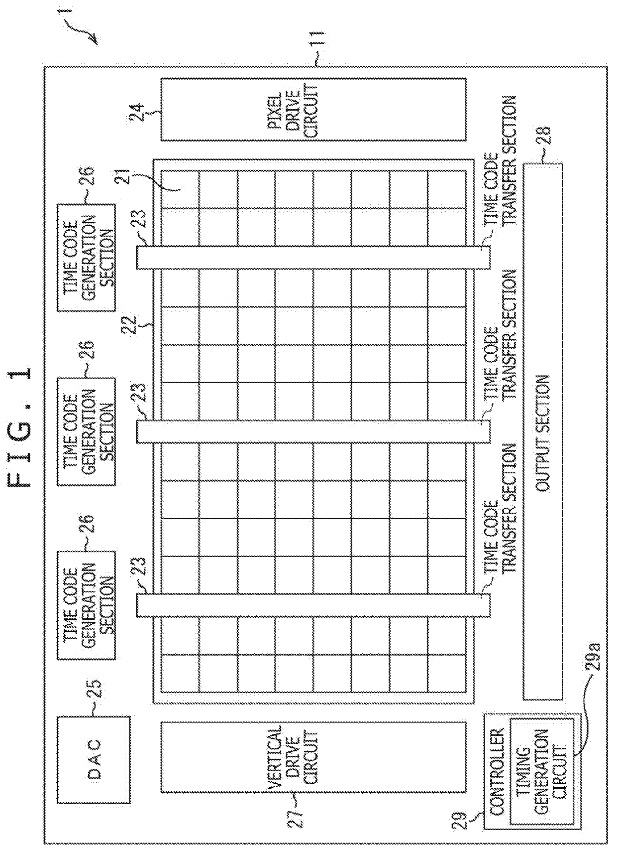
[0041]1. Schematic exemplary configuration of the solid-state imaging apparatus

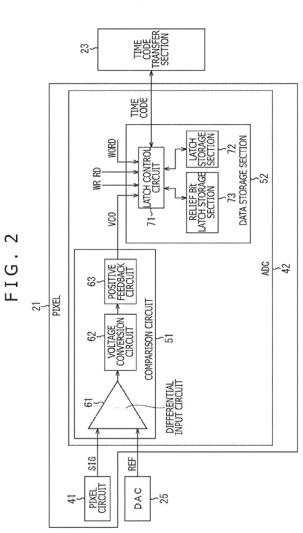
[0042]2. Detailed exemplary configuration of the pixel

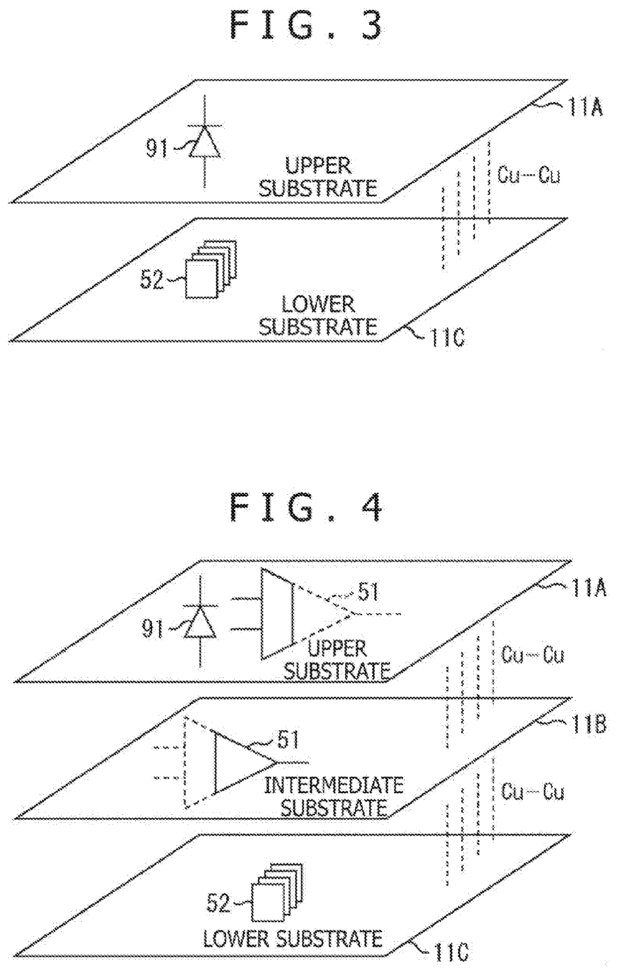
[0043]3. Multiple-substrate configuration 1

[0044]4. Multiple-substrate configuration 2

[0045]5. Detailed configuration for controlling the time code transfer section

[0046]6. Detailed exemplary configuration of the data line selection circuit

[0047]7. Exemplary configuration of the time code transfer section

[0048]8. Exemplary configuration of the determination circuit and the ERR information storage latch

[0049]9. Failure detection...


PUM


Abstract

This disclosure relates to an imaging element, an imaging element control method, an imaging apparatus, and an electronic device adapted to suppress the drop in yield of the imaging element with an ever-higher density of circuitry. Multiple transfer paths are configured to transfer, bit by bit, a time code of a predetermined number of bits for use in converting into a digital signal a pixel signal reflecting the intensity of light received by a pixel. The transfer paths are provided with a relief transfer path that is switched for use in the case where an error has occurred on the multiple transfer paths. This disclosure may be applied to the imaging element.

Description

TECHNICAL FIELD[0001]The present disclosure relates to an imaging element, an imaging element control method, an imaging apparatus, and an electronic device. More particularly, the disclosure relates to an imaging element, an imaging element control method, an imaging apparatus, and an electronic device adapted to boost yield.BACKGROUND ART[0002]The method of reading a signal from an imaging element may involve, for example, performing AD conversion (Analog-Digital conversion) in a limited area such as inside a pixel. For such a case, an integration type (slope type) AD conversion method that configures a comparator and a downstream digital circuit has been proposed as a method for providing high area efficiency.[0003]A circuit configuration in which a slope signal is input multiple times to the comparator, with the downstream digital circuit used as a DRAM (Dynamic Random Access Memory), is well known as an exemplary technique for implementing the AD conversion in the limited area ...

Claims


Application Information

Patent Timeline
IPC IPC(8): H04N5/378H04N5/376H04N5/369
CPCH04N25/767H04N25/772H04N25/79H04N25/77H04N25/75H04N25/745
Inventor HONDA, KATSUMI
Owner SONY SEMICON SOLUTIONS CORP
Why Eureka
Try Eureka