Image data processing circuit and image data processing method

a technology of image data and processing circuit, applied in the field of image data processing circuit and image data processing method, can solve the problems of circuit failure to deal, ob correction cannot be performed sufficiently, ob correction precision deterioration

Inactive Publication Date: 2007-06-21
SOCIONEXT INC
View PDF7 Cites 18 Cited by
  • Summary
  • Abstract
  • Description
  • Claims
  • Application Information

AI Technical Summary

Benefits of technology

[0013] By the subtracting process, the value of the dark current component signal and the value of the dark current component included in the pixel signal can be corrected according to the reference dark current component signal. As a result, the value of the dark current component can be set to a predetermined value. That is, occurrence of, for example, line dependency such that the dark current increases / decreases according to increase in the number of lines and variations among lines in the value of the dark current component signal and the value of the dark current component included in the pixel signal can be suppressed. Consequently, at a later image process stage, variations among lines and line dependency do not occur and the dark current component signal can be eliminated from the pixel signal. Thus, the reference signal level corresponding to black in an image can be determined with high precision, and all of pixel signals can be corrected with the determined reference signal level.

Problems solved by technology

In the case where the signal level in the OB area changes more than the clamp level +1 or −1 between lines, a situation that OB correction cannot be performed sufficiently occurs and it is a problem.
Also in the case where the signal level of the OB area changes within the clamp level, the precision of OB correction deteriorates and it is a problem.
When the interval of updating the clamp level is narrowed (for example, to ±0.5) in order to increase precision of OB correction, a correctable range is narrowed, a situation occurs that the circuit cannot deal with the case where the clamp level difference between lines is large, and this is a problem.
There is another problem such that the line dependency as a characteristic that the signal level of the OB area changes on the line unit basis appears more conspicuously as the number of pixels of the CCD increases.
When the signal level of the OB area has the line dependency, at the time of subtracting the clamp level obtained by measuring the signal level of the OB area in a later image process, a situation that the dark current component cannot be completely eliminated occurs.

Method used


Image

  • Image data processing circuit and image data processing method
  • Image data processing circuit and image data processing method
  • Image data processing circuit and image data processing method

Examples


first embodiment

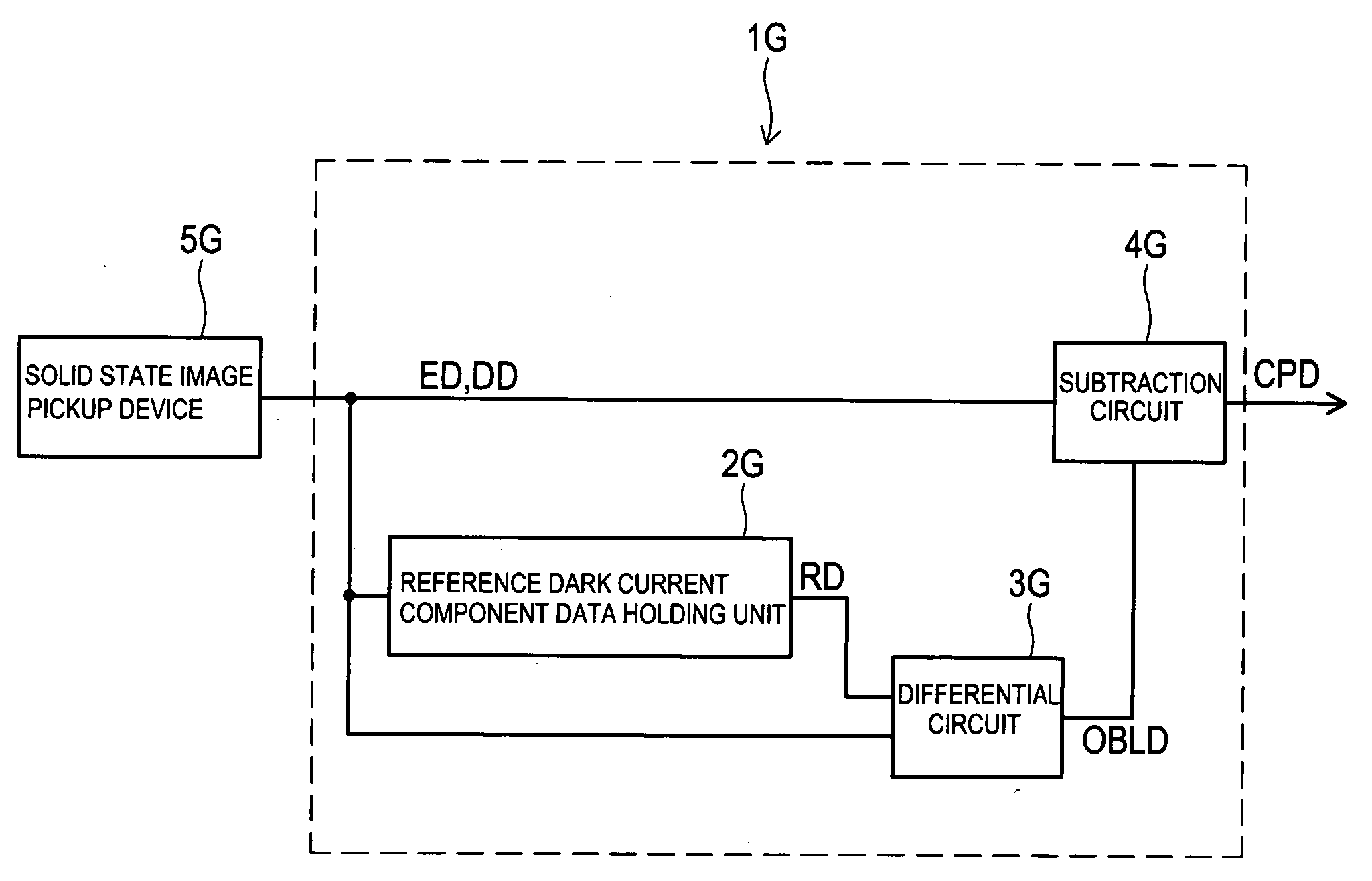
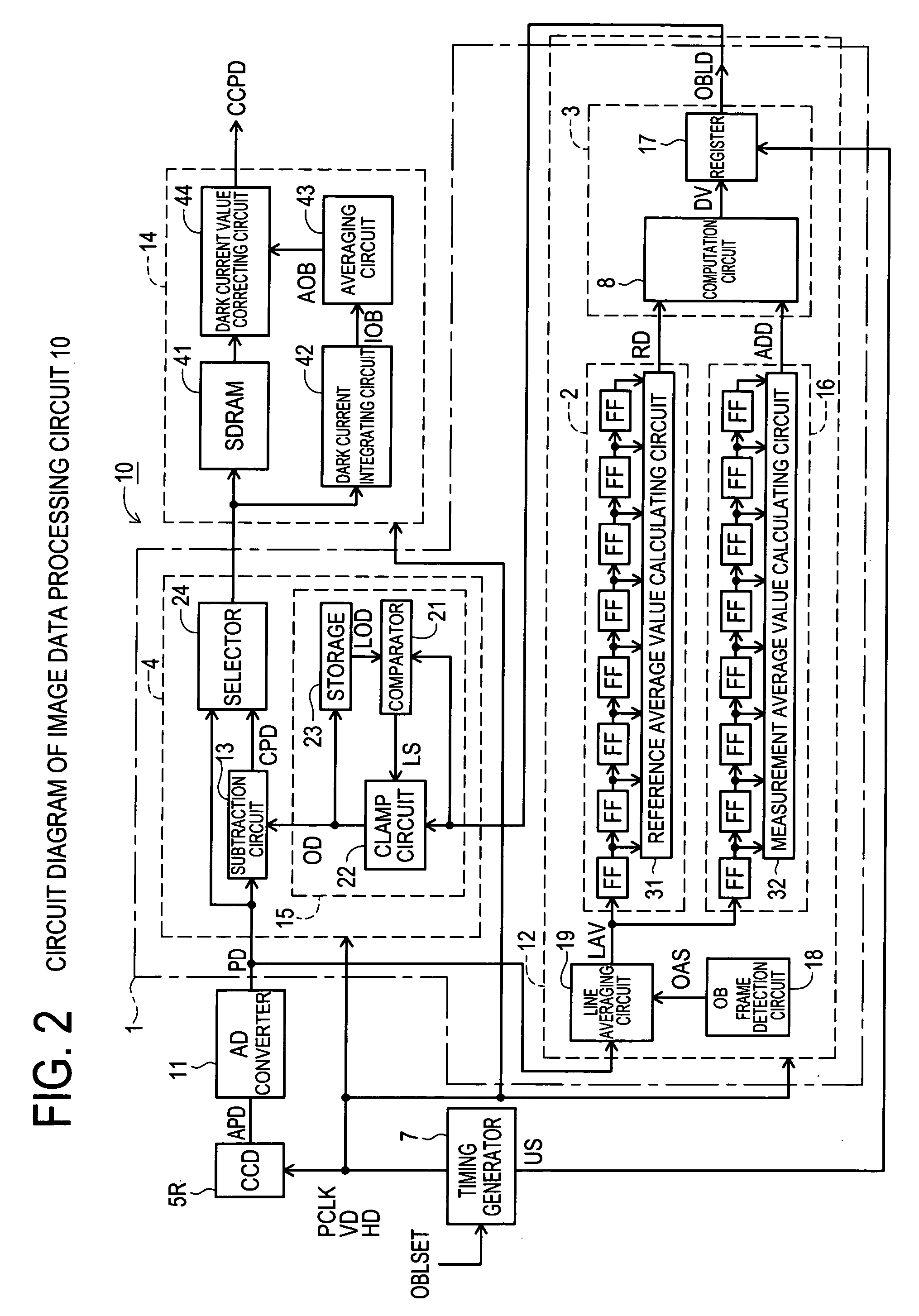
[0030] An image data processing circuit 10 according to the invention will be described by referring to FIG. 2. The image data processing circuit 10 has a CCD sensor 5R of R fields, a timing generator 7, an AD converter 11, a correction circuit 1, and a frame OB correcting unit 14. The correction circuit 1 has a detector 12 and a line OB correcting unit 4.

[0031]FIG. 3 shows R fields in the interlace CCD sensor SR. In the CCD sensor 5R, for convenience of explanation, it is assumed that the number of lines is 20 and there are eight pixels per line. The effective area EA and the OB area OA are pre-set in the CCD sensor 5R by a not-shown register. The effective area EA is an area for obtaining the effective pixel data ED. The OB area OA is an OB (Optical Black) part as a shielded pixel area and is an area for obtaining the dark current component data DD. The CCD sensor 5R outputs analog pixel data APD. The AD converter 11 converts the analog pixel data APD to digital data, and outputs ...

second embodiment

[0059] An image data processing circuit 10a according to the invention will be described with reference to FIG. 7. The image data processing circuit 10a has, in addition to the components of the image data processing circuit 10 shown in FIG. 2, an analog subtraction circuit 51 and an analog front end selector 25. By the analog subtraction circuit 51, the analog front end selector 25, and the AD converter 11, an analog front end 52 is formed. To the analog subtraction circuit 51, the analog pixel data APD output from the CCD sensor 5R and a detection value OBLD output from the register 17 are entered. To the analog front end selector 25, a correction permit signal OBLEN2, subtracted pixel data SPD which is output from the analog subtraction circuit 51, and the analog pixel data APD output from the CCD sensor 5R is entered. The output of the analog front end selector 25 is entered to the AD converter 11. To the register 17, the update signal US is entered every four counts of a line c...


PUM


Abstract

An object of the present invention is to provide an image data processing circuit and an image data processing method capable of determining a reference signal level corresponding to black in an image with high precision by suppressing occurrence of line dependency and the like in a dark current component signal included in image data output from a solid state image pickup device. A reference dark current component data holding unit selects a reference line from a solid state image pickup device and holds a dark current component of the reference line as a head line average value. To a subtraction circuit, dark current component data and effective pixel data is sequentially input on the line unit basis. A differential circuit obtains, as a detection value, a change amount with respect to the head line average value, of the dark current component data included in a preceding line. The subtraction circuit subtracts the detection value from the dark current component data and the effective pixel data entered.

Description

CROSS-REFERENCE TO RELATED APPLICATIONS [0001] This application is based upon and claims the benefit of priority from each of the prior Japanese Patent Application No. 2005-363741 filed on Dec. 16, 2005, the entire contents of which are incorporated herein by reference. BACKGROUND OF THE INVENTION [0002] 1. Field of the Invention [0003] The present invention relates to an image data processing circuit and an image data processing method. More particularly, the invention relates to an image process suitable for correcting an optical black part in an output of a solid state image pickup device such as a digital still camera or a digital video camera. [0004] 2. Description of Related Art [0005] In a video camera and the like, a CCD (Charge Coupled Device) is used as an image pickup device. An output of the CCD includes not only a photoelectric conversion output generated when light falls on the photosensitive surface of the CCD but also a component of dark current which occurs even whe...

Claims


Application Information

Patent Timeline
Patent Type & Authority Applications(United States)
IPC IPC(8): H04N9/64H04N1/028H04N1/407H04N5/335H04N5/351H04N5/361H04N5/365H04N5/369H04N5/372H04N5/378H04N9/07
CPCH04N5/361H04N25/63H04N23/80H04N25/772
Inventor OHARA, KUNIHIROFUKUOKA, TOMOHIRO
Owner SOCIONEXT INC
Why Eureka
Try Eureka