Multipath switch circuit, chip and communication terminal

a multi-path switch and communication terminal technology, applied in the field of multi-path switch circuits, chips and communication terminals, can solve the problems of long development period, high cost, and affecting the differential loss so as to achieve the effect of improving the linear characteristics of the switch, improving the performance, and effective improvement of the differential loss of the multi-path antenna switch

Inactive Publication Date: 2019-12-26
VANCHIP TIANJIN TECH
View PDF2 Cites 0 Cited by
  • Summary
  • Abstract
  • Description
  • Claims
  • Application Information

AI Technical Summary

Benefits of technology

[0025](1) based on the existing device processes and switch circuit structures, the differential loss of the multipath antenna switch can be effectively improved by using concise lines and methods, and the linear characteristics of the switch can be further improved by changing the symmetry properties of direct current bias points; and
[0026](2) compared with the conventional design, the chip area may be not additionally occupied while the performance is improved, so that the costs are effectively controlled.

Problems solved by technology

In addition, on one hand, when each switch transistor is connected, there is parasitic capacitance between a source electrode and a gate and between a drain electrode and the gate of the switch transistor.
Consequently, some of radio frequency signals are leaked from the source electrode and the drain electrode to the gate and the differential loss characteristics of the switch are affected.
On the other hand, although currently a lot of semiconductor manufacturers are devoted to the development of novel processes and switch devices, the development period thereof is long and the costs are high.

Method used


Image

  • Multipath switch circuit, chip and communication terminal
  • Multipath switch circuit, chip and communication terminal
  • Multipath switch circuit, chip and communication terminal

Examples


embodiment 1

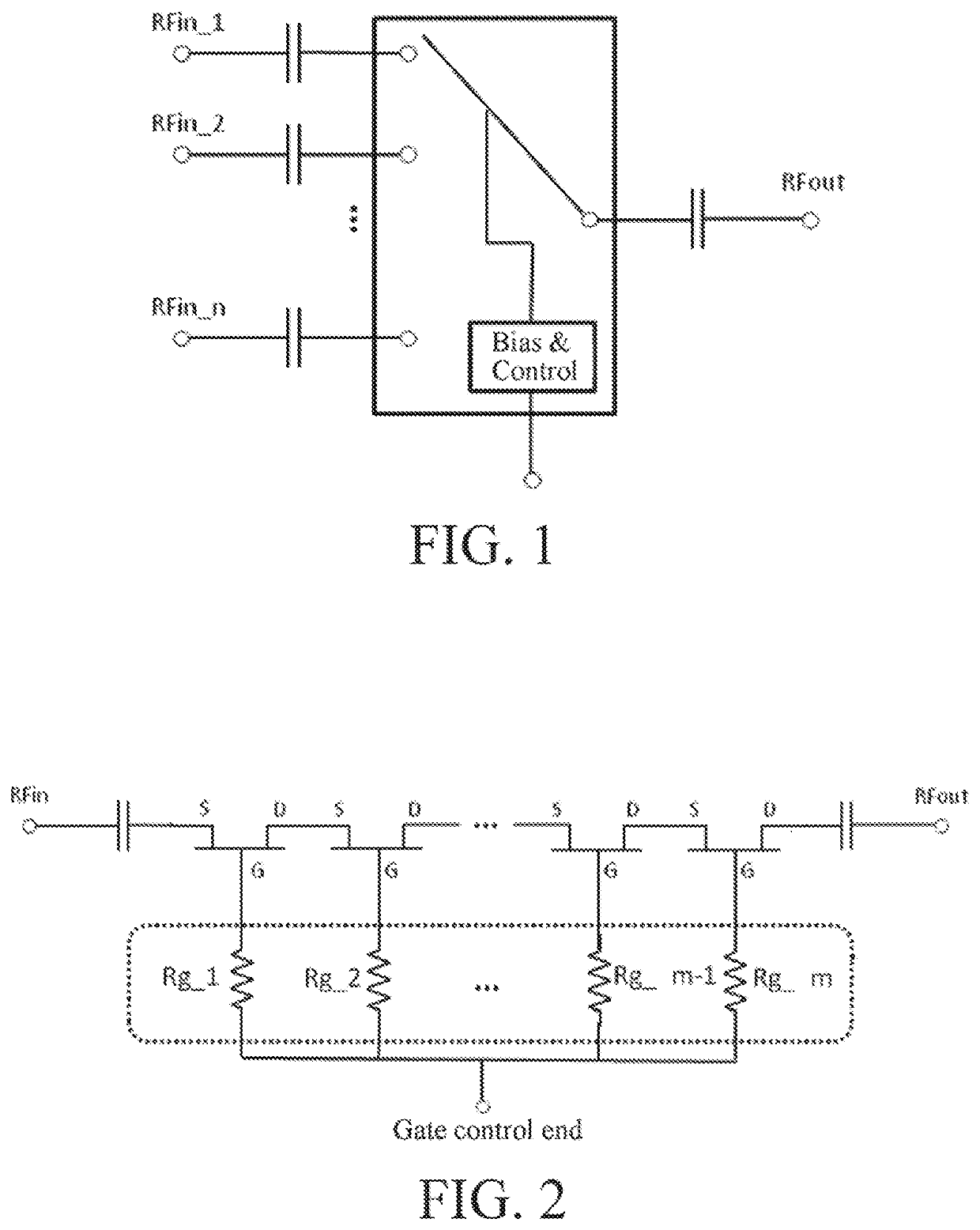
[0035]Referring to FIG. 3, FIG. 3 is a principle diagram of a multipath switch circuit according to Embodiment 1 of the present invention. The multipath switch circuit includes: common gate switch transistor groups that are connected in series, a source-drain bias resistance network 101, and a gate bias resistance network 102.

[0036]In the common gate switch transistor groups, a source electrode of a first switch transistor is connected to a radio frequency signal input end RFin of a switch path by using a DC blocking capacitor, and a drain electrode of a last switch transistor is connected to a radio frequency signal output end RFout of the switch path by using a DC blocking capacitor. Drain electrodes and source electrodes of other adjacent switch transistors in the common gate switch transistor groups are sequentially connected in series.

[0037]The source-drain bias resistance network 101 is disposed between the source electrode of the first switch transistor and the drain electrod...

embodiment 2

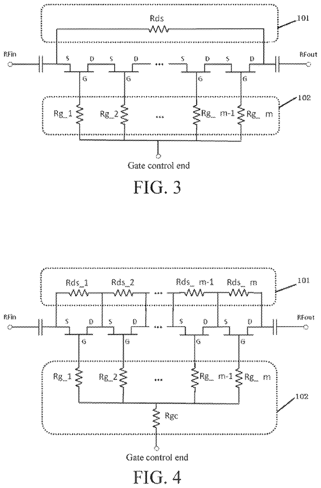
[0040]Referring to FIG. 4, FIG. 4 is a principle diagram of a multipath switch circuit according to Embodiment 2 of the present invention. Similar to Embodiment 1, the multipath switch circuit includes: common gate switch transistor groups that are connected in series, a source-drain bias resistance network 101, and a gate bias resistance network 102. However, for the source-drain bias resistance network 101, the gate bias resistance network 102 is further improved with respect to Embodiment 1.

[0041]The source-drain bias resistance network 101 includes: several resistors (Rds_1, Rds_2, . . . , Rds_m) that have a number the same as that of switch transistors in the common gate switch transistor groups and that have one-to-one correspondence with the switch transistors, where the resistors are disposed between source electrodes and drain electrodes of the corresponding switch transistors in a parallel manner and are sequentially connected in series.

[0042]The gate bias resistance netwo...

embodiment 3

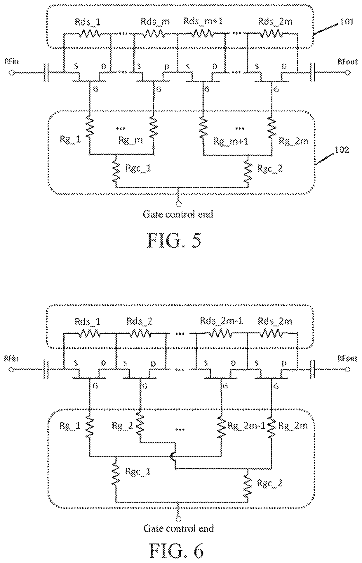
[0044]Referring to FIG. 5, FIG. 5 is a principle diagram of a multipath switch circuit according to Embodiment 3 of the present invention. Similar to Embodiment 2, the multipath switch circuit includes: common gate switch transistor groups that are connected in series, a source-drain bias resistance network 101, and a gate bias resistance network 102. However, the gate bias resistance network 102 is further improved with respect to Embodiment 2.

[0045]The gate bias resistance network 102 includes: several separate gate bias resistors Rg_1, . . . , Rg_m, Rg_m+1, . . . , Rg_2m that have a number the same as that (2m) of switch transistors in the common gate switch transistor groups and that have one-to-one correspondence with the switch transistors, and a first common gate bias resistor Rgc_1 and a second common gate bias resistor Rgc_2. One end of each separate gate bias resistor is connected to a gate of a corresponding switch transistor, and the several separate gate bias resistors ...


PUM


Abstract

A multipath switch circuit, a chip comprising the multipath switch circuit, and a communication terminal comprising the multipath switch circuit or the chip. The multipath switch circuit is applied to a solid antenna switch, comprising common gate switch transistor groups which are connected in series and arranged between a radio frequency signal input end (RFin) and a signal output end (RFout), and a source-drain bias resistance network (101) which is arranged between a source electrode (S) of the first switch transistor connected to the signal input end (RFin) and a drain electrode (D) of the last switch transistor connected to the signal output end (RFout).

Description

BACKGROUNDTechnical Field[0001]The present invention relates to a multipath switch circuit used in a solid antenna switch, a chip including the multipath switch circuit, and a communication terminal, and belongs to the field of integrated circuit technologies.Related Art[0002]Currently, solid antenna switches have been widely applied to wireless communication front end modules or multipath antenna switch modules. In rapidly developed multimode and multiband smartphone systems, the number of modes thereof and the number of bands thereof are constantly increasing. This requires for an increasing number of paths in antenna switches, and the differential loss and linear characteristics thereof also need to be kept or even improved.[0003]In the prior art, a structural block diagram of a typical multipath antenna switch is shown in FIG. 1. When a switch of one of the paths is connected, switches of other paths are simultaneously disconnected. In this way, only a radio frequency signal con...

Claims


Application Information

Patent Timeline
Patent Type & Authority Applications(United States)
IPC IPC(8): H04B1/00H03K17/94H04B1/10
CPCH03K17/94H03K17/693H03K2217/0054H04B1/006H04B1/1081
Inventor LIN, SHENG
Owner VANCHIP TIANJIN TECH
Why Eureka
Try Eureka