High-speed electroplating method

a high-speed electroplating and electrodeposition technology, applied in the field of electroplating methods, can solve the problems of non-uniform electrodeposition and microstructure, such as grain size, non-uniform grain size,

Inactive Publication Date: 2020-02-13
YUAN ZE UNIV
View PDF9 Cites 2 Cited by
  • Summary
  • Abstract
  • Description
  • Claims
  • Application Information

AI Technical Summary

Benefits of technology

[0013]By aforementioned technology means, the present inventi

Problems solved by technology

Unfortunately, the traditional high-speed electroplating method might result in non-uniform electrodeposition and microstructure, such as gra

Method used


Image

  • High-speed electroplating method
  • High-speed electroplating method
  • High-speed electroplating method

Examples


first embodiment

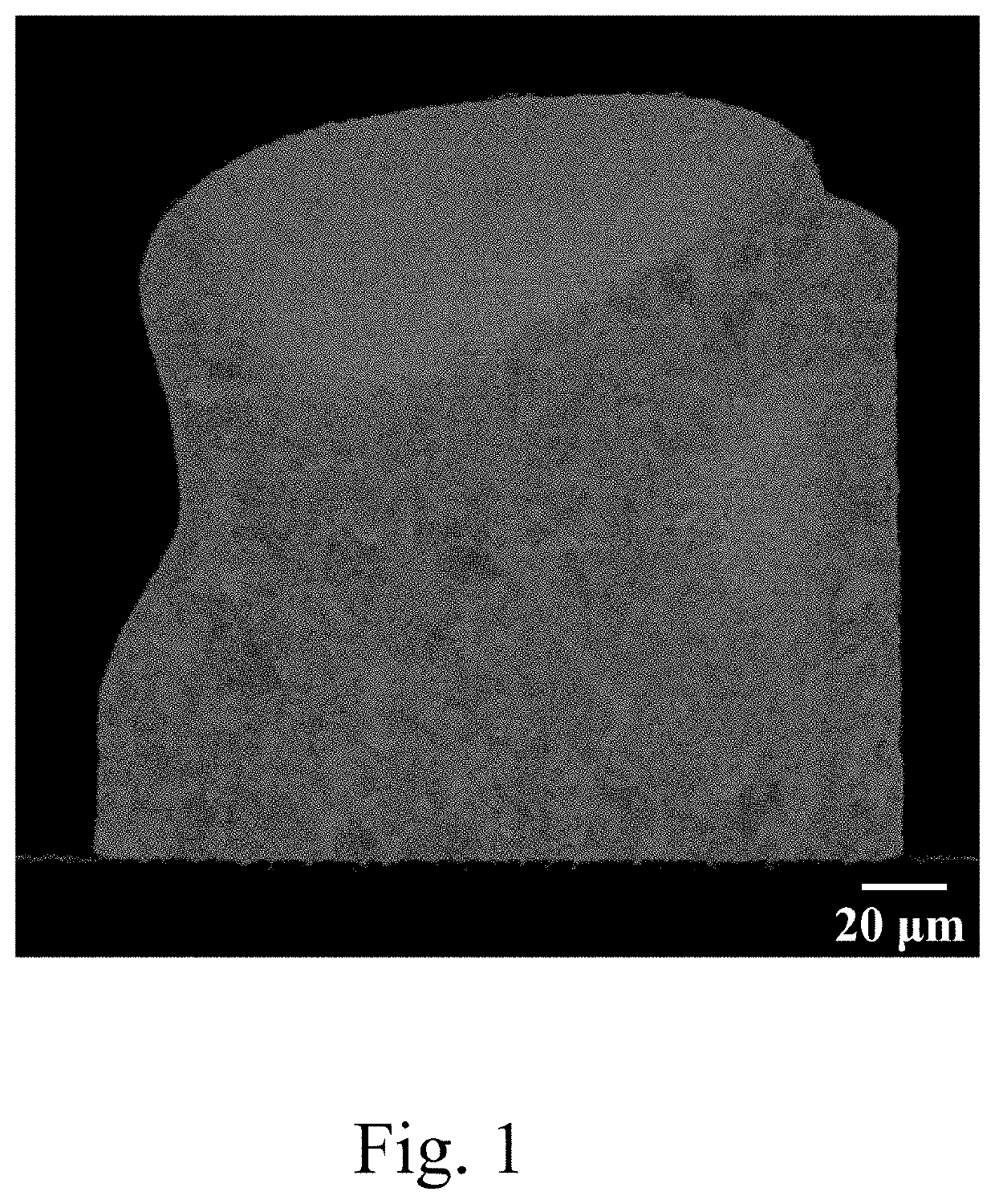
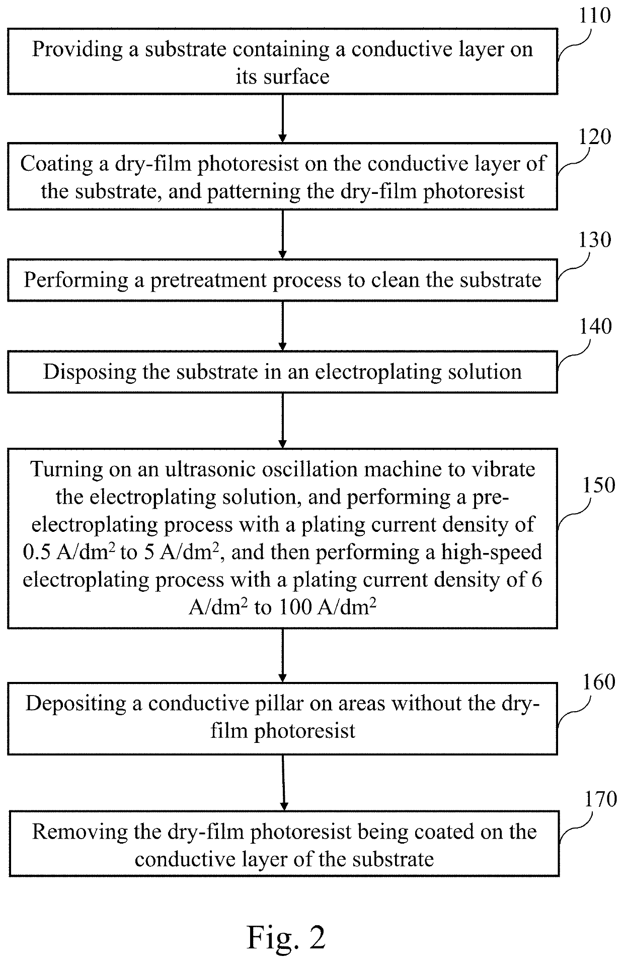
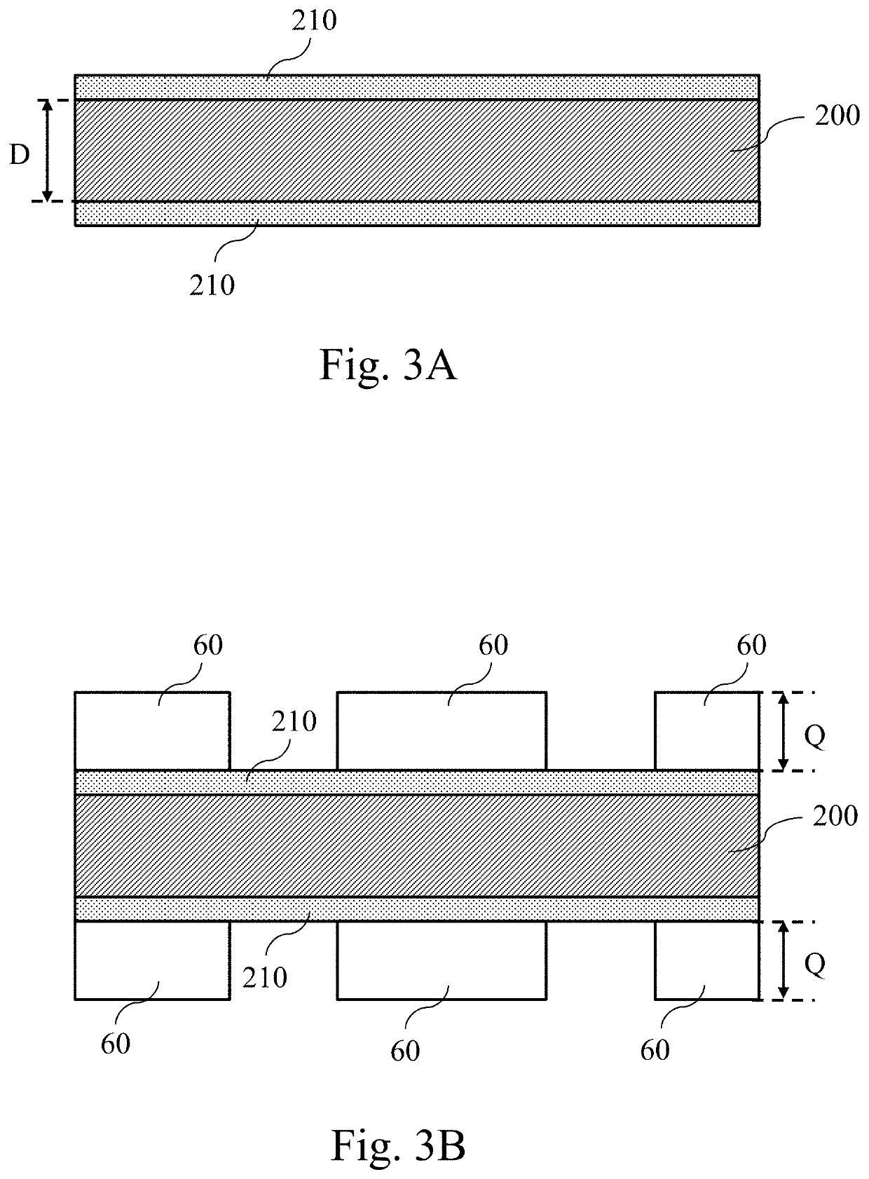
[0040]Please refer to FIG. 2 and FIGS. 3A to 3E, wherein FIG. 2 is a flowchart showing steps for operating a high-speed electroplating method according to the present invention, and FIGS. 3A to 3E are schematic drawings of an embodiment of steps 110, 120, 140 and 150, 160, and 170 of the high-speed electroplating method of FIG. 2. In this embodiment, the high-speed electroplating method includes the following steps: providing a substrate containing a conductive layer on its surface (step 110); coating a dry-film photoresist on the conductive layer of the substrate, and patterning the dry-film photoresist (step 120); performing a pretreatment process to clean the substrate (step 130); disposing the substrate in an electroplating solution (step 140); turning on an ultrasonic oscillation machine to vibrate the electroplating solution, and performing a pre-electroplating process with a plating current density of 0.5 A / dm2 to 5 A / dm2, and then performing a high-speed electroplating proce...

second embodiment

[0051]Please refer to FIG. 5, which is a flowchart showing steps for operating a high-speed electroplating method according to the present invention, the high-speed electroplating method includes the following steps: providing a substrate containing a conductive layer on its surface (step 110); coating a dry-film photoresist on the conductive layer of the substrate, and patterning the dry-film photoresist (step 120); performing a pretreatment process to clean the substrate (step 130); disposing the substrate in an electroplating solution (step 140); turning on an ultrasonic oscillation machine to vibrate the electroplating solution, and turning on a jet flow device to agitate the electroplating solution, and performing a pre-electroplating process with a plating current density of 0.5 A / dm2 to 5 A / dm2, and then performing a high-speed electroplating process with a plating current density of 6 A / dm2 to 100 A / dm2 (step 350); depositing a conductive pillar on areas without the dry-film...

third embodiment

[0056]The high-speed electroplating method of the present invention may be used to form the above-mentioned conductive pillars, and further used to fill the blind-hole structure or the through-hole structure. For details, please refer to FIG. 8 to FIG. 10B, wherein FIG. 8 is a flowchart showing steps for operating a high-speed electroplating method according to the present invention, FIG. 9A is a schematic drawing of an embodiment of a blind-hole structure of step 420 of FIG. 8, FIG. 9B is a schematic drawing of an embodiment of a through-hole structure of step 420 of FIG. 8, FIG. 10A is a schematic drawing of an embodiment of a blind-hole filling via the blind-hole structure of step 460 of FIG. 8, and FIG. 10B is a schematic drawing of an embodiment of a through-hole filling via the through-hole structure of step 460 of FIG. 8. In the embodiment, the high-speed electroplating method includes the following steps: providing a substrate (step 410); forming a blind-hole structure or a ...


PUM

PropertyMeasurementUnit
Frequencyaaaaaaaaaa
Current densityaaaaaaaaaa

Abstract

A high-speed electroplating method is provided. The high-speed electroplating method includes the following steps: providing a substrate containing a conductive layer on its surface; coating a dry-film photoresist on the conductive layer of the substrate, and patterning the dry-film photoresist; performing a pretreatment process to clean the substrate; disposing the substrate in an electroplating solution; turning on an ultrasonic oscillation machine to vibrate the electroplating solution, and turning on a jet flow device to agitate the electroplating solution, and performing a pre-electroplating process with a plating current density of 0.5 A/dm2 to 5 A/dm2, and then performing a high-speed electroplating process with a plating current density of 6 A/dm2 to 100 A/dm2; depositing a conductive pillar on areas without the dry-film photoresist; and removing the dry-film photoresist being coated on the conductive layer of the substrate. Thus, the high-speed electroplating method can achieve high-speed electrodeposition with uniform microstructures.

Description

CROSS-REFERENCE STATEMENT[0001]All related applications are incorporated by reference[0002]The present application is based on, and claims priority from, Taiwan Application Serial Number 107127821, filed Aug. 9, 2018, the disclosure of which is hereby incorporated by reference herein in its entirety.BACKGROUNDTechnical Field[0003]The invention relates to an electroplating method. In particular, the invention pertains to a high-speed electrodeposition enhanced by ultrasonic oscillation.Related Art[0004]With the trend of thinner, lighter, and more multifunctional, the microelectronic products are urgently needed to increase the device quantity through the stacking package technique in recent years.[0005]In the design of stacking packages, each wiring layer of different packaging levels needs to be connected with each other to achieve electrical conduction. To meet such requirements, some manufacturing methods are provided, for example, depositing a conductive pillar between two differ...

Claims


Application Information

Patent Timeline
IPC IPC(8): C25D5/08C25D5/02C25D21/10C25D5/34
CPCC25D5/34C25D21/10C25D5/022C25D5/08C25D3/46C25D3/48C25D3/12C25D3/38C25D3/50C25D7/00C25D5/20C25D5/617
Inventor HO, CHENG ENHUANG, BAU CHINWU, YU KUNYANG, CHENG HSIEN
Owner YUAN ZE UNIV
Why Eureka
Try Eureka